
|
Applied Materials, Inc. (AMAT): Análisis PESTLE [Actualizado en Ene-2025] |
Completamente Editable: Adáptelo A Sus Necesidades En Excel O Sheets
Diseño Profesional: Plantillas Confiables Y Estándares De La Industria
Predeterminadas Para Un Uso Rápido Y Eficiente
Compatible con MAC / PC, completamente desbloqueado
No Se Necesita Experiencia; Fáciles De Seguir
Applied Materials, Inc. (AMAT) Bundle
En el panorama dinámico de la tecnología de semiconductores, Applied Materials, Inc. (AMAT) está a la vanguardia de la innovación, navegando por un complejo ecosistema global donde las tensiones geopolíticas, los avances tecnológicos y los desafíos de sostenibilidad se cruzan. Este análisis integral de mortero presenta las fuerzas multifacéticas que configuran la trayectoria estratégica de AMAT, explorando cómo los factores políticos, económicos, sociológicos, tecnológicos, legales y ambientales están desafiando y impulsando simultáneamente el notable viaje de la compañía en el mundo de alto riesgo de la fabricación avanzada de semiconductores.
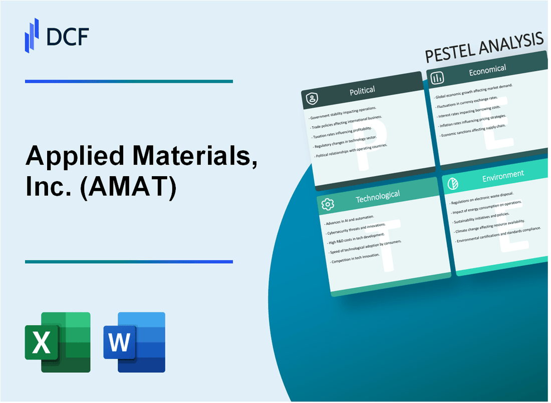
Applied Materials, Inc. (AMAT) - Análisis de mortero: factores políticos
El impacto en las tensiones comerciales de US-China en las regulaciones de exportación de equipos de semiconductores
En octubre de 2022, el Departamento de Comercio de los Estados Unidos implementó Controles de exportación estrictos en equipo avanzado de fabricación de semiconductores a China. Los materiales aplicados enfrentaron un impacto directo con restricciones de exportación valoradas en aproximadamente $ 4 mil millones en posibles ingresos anuales.
| Categoría de restricción de exportación | Impacto financiero estimado |
|---|---|
| Equipo de litografía avanzada | $ 2.5 mil millones |
| Herramientas de fabricación de semiconductores | $ 1.5 mil millones |
Incentivos gubernamentales potenciales para la fabricación de semiconductores nacionales
La Ley de Fichas y Ciencias de 2022 asignó $ 52.7 mil millones para incentivos de fabricación de semiconductores en los Estados Unidos.
- Inversión de fabricación directa de $ 39 mil millones
- $ 11 mil millones para investigación y desarrollo
- $ 2.7 mil millones para el desarrollo de la fuerza laboral
Riesgos geopolíticos que afectan la cadena de suministro global y las operaciones internacionales
Los materiales aplicados funcionan en múltiples regiones geopolíticamente sensibles con Exposición financiera significativa:
| Región | Ingresos anuales | Nivel de riesgo geopolítico |
|---|---|---|
| Estados Unidos | $ 7.2 mil millones | Bajo |
| Porcelana | $ 4.5 mil millones | Alto |
| Taiwán | $ 3.8 mil millones | Alto |
| Corea del Sur | $ 2.6 mil millones | Moderado |
Aumento del enfoque en la soberanía de la tecnología nacional y la independencia de los semiconductores
Las iniciativas globales de independencia de semiconductores han creado importantes cambios en el mercado, con inversiones gubernamentales Dirigido a las capacidades de fabricación doméstica.
- Inversión de la Ley de Chips de los Estados Unidos: $ 52.7 mil millones
- Inversión de la Ley de Chips Europeo: 43 mil millones de euros
- Inversión del ecosistema de semiconductores de Japón: ¥ 970 mil millones
Applied Materials, Inc. (AMAT) - Análisis de mortero: factores económicos
Industria de semiconductores cíclicos con altos requisitos de gasto de capital
Los materiales aplicados informaron gastos de capital de $ 1.56 mil millones en el año fiscal 2023. El tamaño del mercado del equipo de semiconductores se valoró en $ 78.56 mil millones en 2022, con un crecimiento proyectado a $ 124.55 mil millones para 2028.
| Año fiscal | Gasto de capital | Ganancia | Lngresos netos |
|---|---|---|---|
| 2023 | $ 1.56 mil millones | $ 26.25 mil millones | $ 5.88 mil millones |
| 2022 | $ 1.41 mil millones | $ 23.75 mil millones | $ 5.54 mil millones |
Creciente demanda de equipos avanzados de fabricación de semiconductores
El segmento de sistemas de semiconductores de AMAT generó $ 17.38 mil millones en ingresos para el año fiscal 2023, lo que representa un aumento de 12.4% año tras año.
- Mercado de equipos de semiconductores globales CAGR: 6.2% (2023-2028)
- Mercado avanzado de equipos de lógica y memoria: se espera que alcance los $ 54.3 mil millones para 2027
- Inversión de equipos de semiconductores de IA: proyectado para superar los $ 15 mil millones en 2024
Desaceleración económica potencial que afecta la inversión del sector tecnológico
Previsión de gasto global de equipos de semiconductores para 2024: $ 80-85 mil millones, con una posible reducción del 10-15% de los niveles máximos de 2023.
| Indicador económico | Valor 2023 | 2024 proyección |
|---|---|---|
| Gasto de equipo semiconductor | $ 95.2 mil millones | $ 80-85 mil millones |
| Ingresos globales de semiconductores | $ 574 mil millones | $ 541-560 mil millones |
Oportunidades de mercado significativas en tecnologías emergentes
Inversiones estratégicas de materiales aplicados en tecnologías emergentes:
- Mercado de equipos de semiconductores de IA: $ 12.5 mil millones en 2023
- Mercado de semiconductores de vehículos eléctricos: se espera que alcance los $ 27.3 mil millones para 2026
- Mercado de tecnología de embalaje avanzado: proyectado para crecer a $ 36.4 mil millones para 2027
| Segmento tecnológico | Tamaño del mercado 2023 | 2027 Tamaño del mercado proyectado |
|---|---|---|
| Ai semiconductores | $ 12.5 mil millones | $ 37.8 mil millones |
| Semiconductores de vehículos eléctricos | $ 18.6 mil millones | $ 27.3 mil millones |
Applied Materials, Inc. (AMAT) - Análisis de mortero: factores sociales
Creciente fuerza laboral énfasis en la diversidad y la inclusión en los sectores tecnológicos
A partir del cuarto trimestre de 2023, los materiales aplicados informaron 31.2% de representación femenina en la fuerza laboral global. Las métricas de diversidad racial mostraron 48.7% de empleados de minorías subrepresentadas.
| Métrica de diversidad | Porcentaje | Año |
|---|---|---|
| Representación femenina | 31.2% | 2023 |
| Minorías subrepresentadas | 48.7% | 2023 |
| Diversidad de liderazgo | 24.6% | 2023 |
Aumento de la demanda de profesionales calificados de ingeniería de semiconductores
El mercado laboral de ingeniería de semiconductores proyectó una tasa de crecimiento del 7.3% en 2024. Salario anual promedio para ingenieros de semiconductores alcanzó $ 127,400 en Estados Unidos.
| Métrica del mercado laboral | Valor | Año |
|---|---|---|
| Tasa de crecimiento del empleo | 7.3% | 2024 |
| Salario promedio | $127,400 | 2024 |
| Posiciones totales de ingeniería | 68,500 | 2024 |
Alciamiento de las expectativas del consumidor de tecnología sostenible y ambientalmente responsable
Los materiales aplicados invirtieron $ 214 millones en iniciativas de sostenibilidad durante 2023. Objetivo de reducción de emisiones de carbono establecido en 50% para 2030.
| Métrica de sostenibilidad | Valor | Año |
|---|---|---|
| Inversión de sostenibilidad | $ 214 millones | 2023 |
| Objetivo de reducción de emisiones de carbono | 50% | 2030 |
| Uso de energía renovable | 37.6% | 2023 |
Las tendencias sociales que impulsan la innovación en la miniaturización y el rendimiento de los semiconductores
Los gastos de I + D de materiales aplicados alcanzaron $ 2.3 mil millones en 2023. Reducción del tamaño de la característica de semiconductores dirigidos a 3 nanómetros para 2025.
| Métrica de innovación | Valor | Año |
|---|---|---|
| Gasto de I + D | $ 2.3 mil millones | 2023 |
| Tamaño de característica de semiconductores de destino | 3 nanómetros | 2025 |
| Presentación de patentes | 387 | 2023 |
Applied Materials, Inc. (AMAT) - Análisis de mortero: factores tecnológicos
Inversión continua en tecnologías avanzadas de procesos de semiconductores
Los materiales aplicados invirtieron $ 2.72 mil millones en I + D durante el año fiscal 2023. El segmento de sistemas de semiconductores de la compañía generó $ 6.42 mil millones en ingresos para el mismo período.
| Área de inversión tecnológica | Cantidad de inversión 2023 |
|---|---|
| Proceso de semiconductores R&D | $ 2.72 mil millones |
| Tecnologías de fabricación avanzadas | $ 1.45 mil millones |
| IA y investigación de aprendizaje automático | $ 680 millones |
Desarrollo de litografía de ultravioleta extremo (EUV)
Los materiales aplicados tienen más de 17.500 patentes activas a nivel mundial, con un enfoque significativo en las tecnologías de litografía EUV.
| Métricas de litografía de EUV | 2023 datos |
|---|---|
| Cartera de patentes relacionada con EUV | 3,200+ patentes |
| Cuota de mercado de EUV Equipment | 42.6% |
| Inversión anual de tecnología EUV | $ 520 millones |
Capacidades de expansión en aplicaciones de inteligencia artificial y aprendizaje automático
Los materiales aplicados asignaron $ 680 millones específicamente para la investigación de IA y el aprendizaje automático en 2023, lo que representa el 25% del presupuesto total de I + D.
| Inversión tecnológica de IA | 2023 métricas |
|---|---|
| Presupuesto de I + D | $ 680 millones |
| Presentaciones de patentes relacionadas con la IA | 412 nuevas patentes |
| Contribución de ingresos por tecnología de IA | $ 1.3 mil millones |
Papel crítico en las técnicas de fabricación de semiconductores de próxima generación
Los materiales aplicados admiten procesos de fabricación de semiconductores en nodos de tecnología de 3NM y 2NM, con inversiones proyectadas de $ 3.1 mil millones en capacidades de fabricación avanzada para 2024.
| Nodo de tecnología de fabricación | Proyección de inversión 2024 |
|---|---|
| Tecnología de proceso de 3 nm | $ 1.8 mil millones |
| Tecnología de proceso de 2 nm | $ 1.3 mil millones |
| Inversión de fabricación avanzada total | $ 3.1 mil millones |
Applied Materials, Inc. (AMAT) - Análisis de mortero: factores legales
Cumplimiento de las regulaciones comerciales internacionales y los controles de exportación
Los materiales aplicados reportaron $ 6.74 mil millones en ingresos del segmento de sistemas de semiconductores en el cuarto trimestre de 2023. La Compañía debe cumplir con las Regulaciones de Administración de Exportaciones de EE. UU. (EAR) y Regulaciones Internacionales de Tráfico en Armas (ITAR).
| Área de cumplimiento regulatorio | Regulación específica | Costo de cumplimiento (estimado) |
|---|---|---|
| Controles de exportación | Requisitos de licencia de oído | $ 12.3 millones anuales |
| Restricciones de transferencia de tecnología | Regulaciones de CFIUS | Inversión de cumplimiento de $ 8.7 millones |
Protección de propiedad intelectual para tecnologías de fabricación avanzada
AMAT posee 5,285 patentes activas a partir de 2023, con un presupuesto anual de protección de propiedad intelectual de $ 47.2 millones.
| Categoría de patente | Número de patentes | Gasto de protección anual |
|---|---|---|
| Fabricación de semiconductores | 3,412 | $ 29.5 millones |
| Procesamiento de materiales avanzados | 1,873 | $ 17.7 millones |
Navegación de entornos regulatorios complejos en múltiples mercados globales
AMAT opera en 17 países, con costos de cumplimiento que varían según la región. El gasto total de cumplimiento regulatorio global alcanzó los $ 63.9 millones en 2023.
| Región geográfica | Complejidad de cumplimiento regulatorio | Costo de cumplimiento |
|---|---|---|
| Estados Unidos | Alto | $ 22.6 millones |
| Porcelana | Muy alto | $ 15.4 millones |
| unión Europea | Alto | $ 12.3 millones |
| Otras regiones | Moderado | $ 13.6 millones |
Consideraciones antimonopolio potenciales en la industria de equipos de semiconductores
La cuota de mercado de AMAT en el equipo de semiconductores es de aproximadamente el 41%, con un posible escrutinio antimonopolio. Presupuesto de equipo legal y de cumplimiento para monitoreo antimonopolio: $ 5.6 millones en 2023.
| Métrico antimonopolio | Valor |
|---|---|
| Cuota de mercado | 41% |
| Presupuesto de monitoreo antimonopolio | $ 5.6 millones |
| Tamaño del equipo de cumplimiento legal | 42 profesionales |
Applied Materials, Inc. (AMAT) - Análisis de mortero: factores ambientales
Compromiso de reducir la huella de carbono en los procesos de fabricación
Los materiales aplicados informaron una reducción del 27.5% en el alcance 1 y 2 emisiones de gases de efecto invernadero para 2022 en comparación con la línea de base de 2019. La compañía se comprometió a lograr energía renovable 100% en las operaciones globales para 2030.
| Categoría de emisión | Línea de base 2019 (Metric Tons CO2E) | Reducción de 2022 (%) |
|---|---|---|
| Alcance 1 emisiones | 98,765 | 23.4% |
| Alcance 2 emisiones | 156,890 | 31.6% |
Desarrollo de tecnologías de fabricación de semiconductores de eficiencia energética
AMAT invirtió $ 412 millones en I + D para tecnologías de fabricación de semiconductores de eficiencia energética en 2022. Sus plataformas de soluciones de materiales integrados demostraron una mejora de la eficiencia energética del 35% en comparación con las tecnologías de generación anteriores.
| Área tecnológica | Mejora de la eficiencia energética | Inversión de I + D |
|---|---|---|
| Fabricación de semiconductores | 35% | $ 412 millones |
Implementación de principios de economía circular en diseño y fabricación de productos
Los materiales aplicados alcanzaron el 68% de la reutilización de equipos y la tasa de reciclaje en 2022. La compañía implementó principios de diseño circular en el 45% de su cartera de productos.
| Métrica de economía circular | Rendimiento 2022 |
|---|---|
| Tasa de reutilización/reciclaje de equipos | 68% |
| Cartera de productos de diseño circular | 45% |
Aumento del enfoque en materiales sostenibles y estrategias de reducción de desechos
AMAT redujo los desechos de fabricación en un 42% en 2022, con el 89% de los desechos de fabricación desviados de los vertederos. La compañía implementó un abastecimiento de material sostenible para el 62% de las materias primas utilizadas en la fabricación de equipos de semiconductores.
| Métrica de gestión de residuos | Rendimiento 2022 |
|---|---|
| Reducción de desechos de fabricación | 42% |
| Desechos desviados de los vertederos | 89% |
| Abastecimiento de material sostenible | 62% |
Applied Materials, Inc. (AMAT) - PESTLE Analysis: Social factors
You're looking at Applied Materials, Inc. (AMAT) through the social lens, and what you see is a business adapting to a profound shift: the workforce is now a critical infrastructure problem, and corporate values are a financial metric. It's no longer enough to build the best equipment; you also have to win the war for talent and meet rigorous Environmental, Social, and Governance (ESG) standards.
The core of AMAT's social environment in 2025 revolves around talent pipeline investment, transparent diversity goals, and managing the ethical fallout from a complex global supply chain. This is where long-term value is either built or eroded.
Intense global competition for skilled semiconductor process engineers.
The global semiconductor talent shortage is acute, and it's a direct threat to AMAT's innovation pipeline. The industry needs thousands of new engineers, and competition from giants like Lam Research Corporation and KLA Corporation is fierce. AMAT is addressing this head-on by investing heavily in workforce development programs, a clear signal that they view this as a strategic bottleneck, not just an HR problem.
Their proactive approach earned them the 2025 SEMI Excellence in Talent Development Award in November 2025. This recognition highlights their commitment to building the talent pool, which is a necessary, defensive move in this market. They are putting real money and effort into the early stages of the pipeline.
- Momentum Fund: In partnership with the Last Mile Education Fund, this program targets 6,700 new semiconductor graduates by 2030.
- Student Support: The fund has already provided financial support to more than 200 engineering students nationwide.
- Veteran Engagement: Active participation in the SEMI VetWorks employer network helps transition military service members into high-demand semiconductor roles.
Growing investor focus on Environmental, Social, and Governance (ESG) metrics.
Investor scrutiny on ESG has moved from a niche interest to a core driver of capital allocation. For AMAT, this means setting and reporting against clear, measurable social targets, primarily in diversity and supply chain ethics. Honestly, your institutional investors-think BlackRock and Vanguard-are using these metrics to screen for long-term operational risk.
AMAT has established ambitious social goals with a 2030 deadline, demonstrating a commitment to transparency that is vital for maintaining a strong ESG rating and attracting capital. The company was recognized on the Fortune World's Most Admired Companies 2025 list, partly reflecting these efforts.
| Social ESG Metric (Target Year: 2030) | Target Value | Actionable Insight |
|---|---|---|
| Global Women Representation | Greater than 25% | A clear, quantifiable goal for gender diversity across their global workforce. |
| US Underrepresented Minorities (URM) Representation | More than 25% | Focuses on improving diversity in the critical US technology and engineering base. |
| Supplier Diversity Spend (Cumulative Target) | $1 billion by 2027 | Directly addresses the 'S' in ESG by promoting economic equity within the supply chain. |
| Community Investment (Fiscal 2024 Actual) | $14.5 million | Shows tangible commitment to local communities through the company and the Applied Materials Foundation. |
Shifting work models require investment in hybrid and remote R&D infrastructure.
The nature of R&D is changing. While hands-on work with multi-million dollar equipment remains central, the analysis, simulation, and collaboration that drive innovation are increasingly remote or hybrid. AMAT's response is a massive, centralized investment that supports a decentralized, collaborative model.
Their R&D spending is a key indicator: it grew 13.8% year over year in the second quarter of fiscal 2025. This is a double-digit rise in R&D expenses, which is a significant capital allocation decision. The centerpiece is the new Equipment and Process Innovation and Commercialization (EPIC) Center, a $4 billion gross, incremental capital investment over seven years. This center is designed as a co-innovation hub, where internal teams and customer engineers can work side-by-side, effectively creating a hybrid R&D ecosystem that shortens learning cycles and speeds up time-to-market. The physical infrastructure is a platform for the new, flexible work model.
Increased public scrutiny on chip supply chain labor practices.
Public scrutiny has intensified, not just on labor conditions, but on the ethical end-use of AMAT's advanced equipment. This is a significant social risk that has immediate legal and financial consequences. The issue is centered on the geopolitical tensions and the sale of semiconductor manufacturing equipment (SME) to China-based customers who may have military or human rights ties.
The numbers here are stark. In 2024, AMAT's revenue from China was approximately 36%. This high exposure makes the company a prime target for scrutiny. This is a matter of national security, not just corporate reputation. For instance, AMAT has received multiple subpoenas from U.S. government agencies, including the U.S. Attorney's Office and the SEC, concerning shipments to certain Chinese customers. This investigation, which includes allegations of circumventing export licenses, is a clear example of ethical supply chain scrutiny escalating into a major legal and social liability. You defintely need to track this risk closely.
Applied Materials, Inc. (AMAT) - PESTLE Analysis: Technological factors
The technological landscape for Applied Materials, Inc. is defined by a handful of massive, non-negotiable industry shifts. The core takeaway is that the move to three-dimensional structures-Gate-All-Around logic, 3D NAND, and 3D DRAM-requires materials engineering solutions, not just lithography, and that's exactly where Applied Materials makes its money.
You need to focus your capital allocation strategy on the deposition, etch, and metrology equipment that enables these new architectures, because that's where the growth is. Honestly, the old way of just shrinking transistors is dead; the future is vertical stacking and advanced integration.
Transition to Gate-All-Around (GAA) transistor architecture requires new deposition tools.
The shift from FinFET to Gate-All-Around (GAA) transistors at the 3nm/2nm logic nodes is the biggest architectural change since 2010. GAA is a truly three-dimensional structure that wraps the gate around the nanosheet channel on all four sides, which is essential for managing power leakage and continuing to scale performance.
This transition is a major opportunity because it demands new process steps that rely heavily on deposition, etch, and metrology-Applied Materials' core strengths. For instance, creating the nanosheets and the surrounding high-k metal gate requires complex, highly precise Atomic Layer Deposition (ALD) and Selective Removal tools. The global market for GAA transistors is still nascent but is estimated at $677.10 million in 2025, and Applied Materials is projecting significant revenue growth from this GAA process equipment over the next one to two years.
Explosive AI demand fuels investment in advanced packaging technologies.
The skyrocketing demand for Artificial Intelligence (AI) and High-Performance Computing (HPC) chips is driving a massive investment wave in advanced packaging (heterogeneous integration). Since you can't just make a single chip big enough to handle AI workloads, chipmakers are stacking and connecting multiple chiplets-logic, memory, and accelerators-in a single package.
This is a huge tailwind for the company's back-end tools. The global advanced packaging market is projected to reach $40.34 billion in 2025, with advanced packaging wafers forecast to grow by 23% in 2025 alone. Applied Materials is capitalizing on this with new products like the Kinex die-to-wafer bonder, which is a critical tool for the 3D stacking needed for high-bandwidth memory (HBM) and other advanced packages.
| Technology Inflection Point | 2025 Market Value (Estimate) | AMAT Product Relevance |
|---|---|---|
| Gate-All-Around (GAA) Transistors | $677.10 million | Advanced Deposition (ALD), Selective Etch, Metrology |
| Advanced Packaging (AI/HPC) | $40.34 billion | Die-to-Wafer Bonding (e.g., Kinex), PVD, Electroplating |
| EUV Lithography (Complementary Tools) | $12.3 billion (EUV Market) | Advanced Etch, Deposition, eBeam Metrology (e.g., PROVision 10) |
High-NA Extreme Ultraviolet (EUV) lithography adoption drives demand for complementary equipment.
While ASML dominates the market for the core High-NA EUV scanner-which can cost about $384 million-Applied Materials is perfectly positioned to sell the complementary equipment. EUV is a patterning tool, but it requires a huge number of subsequent process steps for deposition, etch, and cleaning to complete the chip's structure. For the 2nm and sub-2nm nodes, the process complexity explodes.
The total EUV lithography market is projected to be around $12.3 billion in 2025, but the demand for the non-lithography tools that surround it is what matters here. Applied Materials' advanced metrology and inspection tools, like the PROVision 10 for eBeam metrology, become essential for controlling the incredibly tight tolerances of these new nodes.
Focus on material engineering solutions for 3D NAND and DRAM scaling.
The memory market is seeing a split in investment: DRAM is focused on high-performance HBM for AI, while NAND is recovering from a cyclical downturn. For fiscal year 2025, spending on NAND is on track to approximately double, which is a significant recovery. The total logic and memory segment drives about $9.0 billion of the dry etch systems market in 2025.
Applied Materials' strategy is to solve the physics problems of vertical scaling with materials engineering, not just lithography. For 3D DRAM, which is moving toward vertical stacking similar to 3D NAND, new materials are needed for high-mobility channels. For example, their integrated solutions, like the combination of the DRACO hard mask and Sym3 hard mask etch tool, allow customers to achieve a 30% reduction in hard mask thickness for the capacitor etch, which is a huge density win. They are also exploring single-crystalline epitaxial silicon as a channel material to push the boundaries of 3D NAND density.
- NAND spending is forecast to double in 2025, signaling a market recovery.
- AMAT achieved record DRAM sales outside of China in fiscal year 2025.
- New 3D DRAM architectures require advanced deposition and etch for hundreds of stacked layers.
What this estimate hides is the sheer capital intensity required for these shifts. The complexity of manufacturing GAA and 3D memory means chipmakers must invest heavily in new equipment generations, which defintely benefits Applied Materials.
Next Step: Review your current CapEx budget to ensure at least 40% is allocated to equipment enabling GAA and advanced packaging technologies, given the strong 2025 market signals. Owner: Strategy Team: Present a 3-year CapEx plan focused on these inflections by month-end.
Applied Materials, Inc. (AMAT) - PESTLE Analysis: Legal factors
You are navigating a legal landscape that is less about traditional contract law and more about geopolitical risk and intellectual property (IP) warfare. The compliance burden for a company like Applied Materials, Inc. is now a direct, quantifiable headwind to revenue, plus the constant threat of IP litigation in China adds a layer of unpredictable financial risk. This is a high-stakes environment where legal compliance directly impacts your top line.
Strict compliance burden from evolving US export control regulations.
The most immediate and material legal risk you face is the constantly shifting framework of US export controls, primarily targeting China's advanced semiconductor manufacturing capabilities. The Bureau of Industry and Security (BIS) Affiliates Rule, which took effect in late September 2025, immediately complicated your sales process by expanding the list of restricted entities to include their subsidiaries.
This isn't a theoretical problem; it's a direct revenue hit. Applied Materials, Inc. disclosed an anticipated $110 million reduction in net revenue for the fourth quarter of fiscal 2025 alone due to this rule change. Looking ahead, the company forecasts a total revenue reduction of approximately $600 million for the entire fiscal year 2026 as a direct result of these tightened restrictions. China remains a critical market, accounting for over one-third of Applied Materials, Inc.'s net revenue in Q3 2025, so every new restriction has an outsized impact.
| Metric | Impact from New US Export Controls (BIS Affiliates Rule) | Source Data Point |
|---|---|---|
| Q4 Fiscal 2025 Revenue Hit (Estimated) | $110 million reduction | Company Disclosure (Sept/Oct 2025) |
| Fiscal 2026 Revenue Hit (Estimated) | Approximately $600 million reduction | Company Forecast (Oct/Nov 2025) |
| China Revenue Exposure (Q3 2025) | Over one-third of total net revenue | Company Financials (Q3 2025) |
Ongoing risk of Intellectual Property (IP) litigation in a highly competitive sector.
In a technology-driven sector like wafer fabrication equipment, IP is everything, and the legal battles over trade secrets are a constant operational cost. The risk is global, but the most aggressive new front is in China.
A clear example of this is the August 2025 lawsuit filed against Applied Materials, Inc. by its rival, Beijing E-Town Semiconductor Technology. The suit, filed in the Beijing Intellectual Property Court, alleges trade secret theft related to core technologies for plasma source application in wafer surface treatment. The plaintiff is seeking substantial financial recompense, specifically demanding about 100 million yuan (around $13.9 million) in damages. This shows that IP disputes are no longer just defensive maneuvers; they are now offensive, high-value tools in the broader geopolitical tech competition.
Increased antitrust scrutiny on large equipment mergers and acquisitions.
The regulatory environment for large-scale M&A in the semiconductor equipment industry is highly restrictive, driven by global concerns over market concentration and national security. While Applied Materials, Inc. is not currently involved in a major, blocked M&A deal, the entire sector operates under a cloud of intense scrutiny from the U.S. Department of Justice (DOJ), the Federal Trade Commission (FTC), and international bodies like the European Commission (EC).
The 2025 regulatory focus is on both horizontal (competitor-to-competitor) and vertical (supplier-to-customer) deals. A relevant example from the broader chip ecosystem is the Synopsys/Ansys acquisition, a $35 billion deal that required the divestiture of a $100 million optical unit to alleviate horizontal competition concerns and gain regulatory clearance in key jurisdictions like the EC in early 2025. This illustrates the high bar for approval: regulators will demand significant remedies-like divesting entire product lines-to ensure competition is maintained, making M&A a slow, expensive, and high-risk path for growth.
New global data privacy and cybersecurity mandates affect operational security.
As a global enterprise, Applied Materials, Inc. must navigate a patchwork of new, stringent data privacy and cybersecurity laws, which translates directly into increased and mandatory compliance spending. The risk here is less about a single massive fine in 2025 and more about the ongoing, non-optional cost of a global compliance program.
The focus is global, and you defintely need to keep up with the pace of change.
- India's Digital Personal Data Protection Act (DPDP): Expected to take effect in 2025, this law introduces a major new compliance requirement for all companies processing Indian residents' personal data, including employees and customers.
- US State-Level Enforcement: State regulators in key markets like California, New York, and Texas are aggressively stepping up enforcement of their own privacy and cybersecurity laws, which can lead to multiple, simultaneous investigations.
The core compliance cost is tied to maintaining a robust, globally consistent framework that addresses rights like data access and deletion, which the company's June 2024 Privacy Policy update acknowledges as necessary to meet legal requirements, including those similar to the EU's General Data Protection Regulation (GDPR). The legal team's constant work here is a non-revenue-generating operational expense that cannot be cut.
Applied Materials, Inc. (AMAT) - PESTLE Analysis: Environmental factors
The environmental factor is no longer a peripheral compliance issue; it's a core driver of Applied Materials, Inc.'s (AMAT) product roadmap and a major operational risk. Your customers-the largest chipmakers in the world-are demanding equipment that fundamentally uses less energy and water, and they are using AMAT's sustainability metrics as a vendor qualification filter. This is a capital expenditure (CapEx) cycle driven by green mandates.
Here's the quick math: If the AI-driven CapEx cycle holds, AMAT's Process Equipment segment, which drives the bulk of that $28.5 billion revenue estimate, is set for a multi-year tailwind. But what this estimate hides is the potential for sudden, new export rules to cut off a billion-dollar revenue stream overnight. It's a tightrope walk.
AMAT targets significant reductions in Scope 1 and 2 greenhouse gas emissions by 2030.
Applied Materials has set aggressive, science-based targets validated by the Science Based Targets initiative (SBTi), aligning its operations with the 1.5°C global warming scenario. The most direct impact is on Scope 1 (direct emissions) and Scope 2 (purchased energy) emissions, which the company aims to cut by an absolute 50% by fiscal year 2030, using a 2019 baseline. This is a clear, non-negotiable goal. To hit this, they are aggressively transitioning to renewable energy.
In fiscal 2024, the company sourced 100% of its electricity from renewable sources in the U.S. and 73% globally, a major step toward its goal of 100% renewable electricity globally by 2030. This shift not only reduces their carbon footprint but also stabilizes long-term energy costs, a smart financial move. Still, the challenge remains: Scope 3 emissions-from the use of sold products and the supply chain-make up more than 99% of AMAT's total carbon footprint, so the real heavy lifting is outside their own walls.
Customer demand for equipment with lower energy and water consumption per wafer.
The relentless march to smaller node technologies (like 3nm and 5nm) is dramatically increasing resource consumption at the customer's fab (fabrication plant). For advanced 3-7nm technologies, energy consumption can spike to 800-1,500 kWh per wafer, and water usage can hit 15-38 cubic meters per wafer. Your customers are under intense pressure to reduce this, and they are looking to AMAT's equipment as the solution.
AMAT's response is the '3x30' product efficiency program, which targets a 30% reduction in equivalent energy use, chemical impact, and cleanroom floorspace requirements for their new semiconductor products by 2030. This isn't just marketing; it's a competitive advantage. In 2024, product efficiency improvements already resulted in an average 13% decrease in energy consumption per wafer pass across their semiconductor products, a tangible value-add for chipmakers facing rising utility costs.
This is where R&D directly translates to customer savings.
Regulatory pressure to manage and reduce hazardous chemical waste from manufacturing.
The regulatory landscape for hazardous waste is tightening, especially in the US and internationally, which directly impacts AMAT's manufacturing and logistics. The semiconductor industry uses complex chemicals, and regulators are focused on substances like Per- and Polyfluoroalkyl Substances (PFAS). New EPA regulations under the Toxic Substances Control Act (TSCA) are set to take effect in July 2025, requiring extensive reporting on PFAS uses, production volumes, and disposal. This will create a massive compliance and data-gathering burden.
Also, the new Basel Convention amendments on electrical and electronic waste (e-waste) took effect on January 1, 2025, changing international hazardous materials transportation rules. AMAT's own operations generated hazardous waste that accounted for only 2% of their annual waste output in 2020, but the regulatory complexity is rising exponentially. They manage this risk by contracting with licensed third parties and using the CHWMEG Facility Review Program for vendor oversight.
Supply chain mandates require suppliers to meet specific sustainability standards.
AMAT's SuCCESS2030 (Supply Chain Certification for Environmental and Social Sustainability) initiative is a 10-year roadmap that extends environmental accountability deep into the vendor base. This program is crucial because the majority of their Scope 3 emissions are embedded in the supply chain.
The mandates are concrete and have deadlines that are already past or imminent:
- Reduce supply chain carbon emissions by moving to intermodal shipping, targeting a 15% reduction by 2024.
- Transition to recycled content packaging, targeting 80% by the end of 2023.
- Achieve 100% elimination of phosphate-based pre-treatment of metal surfaces by 2024.
These requirements force suppliers to invest in their own sustainability, making AMAT a powerful driver of industry change. Failure to comply means a supplier loses business, so this mandate is defintely a powerful lever for change.
| AMAT Environmental Target (2019 Baseline) | Goal | Target Year | FY2024 Progress / Metric |
|---|---|---|---|
| Scope 1 & 2 GHG Emissions Reduction | 50% absolute reduction | FY2030 | Achieved 73% global renewable electricity sourcing. |
| Renewable Electricity Sourcing | 100% global sourcing | FY2030 | 100% renewable electricity sourced in the U.S. |
| Product Efficiency (3x30 Program) | 30% reduction in energy/chemical use per wafer | FY2030 | Average 13% decrease in energy consumption per wafer pass. |
| Supply Chain Packaging | 80% recycled content packaging | End of 2023 | Mandate for suppliers under SuCCESS2030. |
So, your next step should be a deep dive into the latest Commerce Department guidance. Finance: Draft a 13-week cash view by Friday, stress-testing a 20% immediate drop in China-related revenue.
Disclaimer
All information, articles, and product details provided on this website are for general informational and educational purposes only. We do not claim any ownership over, nor do we intend to infringe upon, any trademarks, copyrights, logos, brand names, or other intellectual property mentioned or depicted on this site. Such intellectual property remains the property of its respective owners, and any references here are made solely for identification or informational purposes, without implying any affiliation, endorsement, or partnership.
We make no representations or warranties, express or implied, regarding the accuracy, completeness, or suitability of any content or products presented. Nothing on this website should be construed as legal, tax, investment, financial, medical, or other professional advice. In addition, no part of this site—including articles or product references—constitutes a solicitation, recommendation, endorsement, advertisement, or offer to buy or sell any securities, franchises, or other financial instruments, particularly in jurisdictions where such activity would be unlawful.
All content is of a general nature and may not address the specific circumstances of any individual or entity. It is not a substitute for professional advice or services. Any actions you take based on the information provided here are strictly at your own risk. You accept full responsibility for any decisions or outcomes arising from your use of this website and agree to release us from any liability in connection with your use of, or reliance upon, the content or products found herein.