
|
Applied Materials, Inc. (AMAT): Analyse de Pestle [Jan-2025 MISE À JOUR] |
Entièrement Modifiable: Adapté À Vos Besoins Dans Excel Ou Sheets
Conception Professionnelle: Modèles Fiables Et Conformes Aux Normes Du Secteur
Pré-Construits Pour Une Utilisation Rapide Et Efficace
Compatible MAC/PC, entièrement débloqué
Aucune Expertise N'Est Requise; Facile À Suivre
Applied Materials, Inc. (AMAT) Bundle
Dans le paysage dynamique de la technologie des semi-conducteurs, Applied Materials, Inc. (AMAT) est à l'avant-garde de l'innovation, naviguant dans un écosystème mondial complexe où les tensions géopolitiques, les percées technologiques et les défis de la durabilité se trouvent. Cette analyse complète du pilon dévoile les forces multiformes qui façonnent la trajectoire stratégique d'Amat, explorant comment les facteurs politiques, économiques, sociologiques, technologiques, juridiques et environnementaux sont simultanément stimulants et propulsant le parcours remarquable de l'entreprise dans le monde à enjeux élevés de la fabrication avancée des semi-conducteurs.
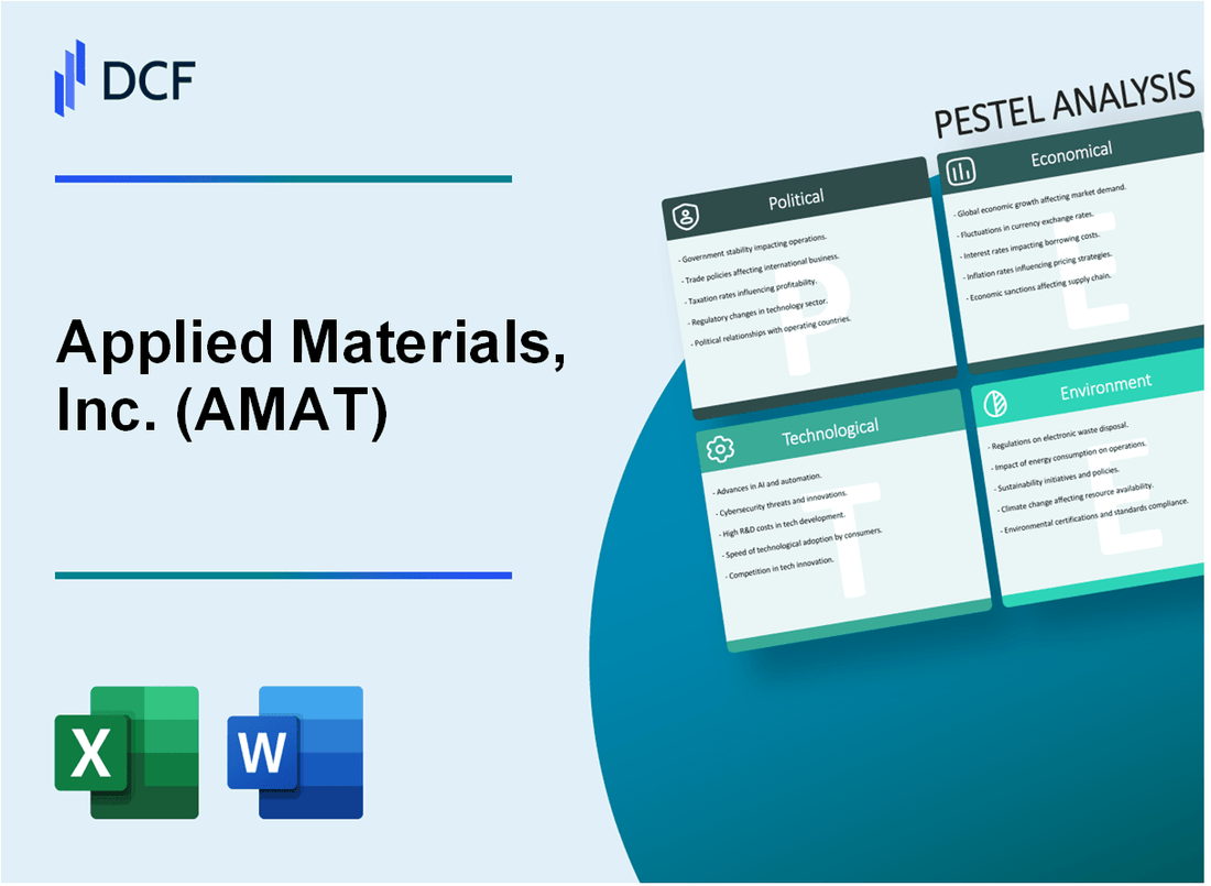
Applied Materials, Inc. (AMAT) - Analyse du pilon: facteurs politiques
Les tensions commerciales américaines-chinoises ont un impact sur les réglementations d'exportation des équipements semi-conducteurs
En octobre 2022, le département américain du commerce a mis en œuvre Contrôles d'exportation stricts sur un équipement de fabrication avancée de semi-conducteurs vers la Chine. Les matériaux appliqués sont confrontés à un impact direct avec des restrictions d'exportation évaluées à approximativement 4 milliards de dollars dans les revenus annuels potentiels.
| Catégorie de restriction d'exportation | Impact financier estimé |
|---|---|
| Équipement de lithographie avancée | 2,5 milliards de dollars |
| Outils de fabrication de semi-conducteurs | 1,5 milliard de dollars |
Incitations potentielles du gouvernement pour la fabrication de semi-conducteurs intérieurs
Le Chips and Science Act de 2022 alloué 52,7 milliards de dollars Pour les incitations de fabrication de semi-conducteurs aux États-Unis.
- 39 milliards de dollars d'investissement de fabrication directe
- 11 milliards de dollars pour la recherche et le développement
- 2,7 milliards de dollars pour le développement de la main-d'œuvre
Risques géopolitiques affectant la chaîne d'approvisionnement mondiale et les opérations internationales
Les matériaux appliqués fonctionnent dans plusieurs régions géopolitiquement sensibles Exposition financière importante:
| Région | Revenus annuels | Niveau de risque géopolitique |
|---|---|---|
| États-Unis | 7,2 milliards de dollars | Faible |
| Chine | 4,5 milliards de dollars | Haut |
| Taïwan | 3,8 milliards de dollars | Haut |
| Corée du Sud | 2,6 milliards de dollars | Modéré |
Accent croissant sur la souveraineté de la technologie nationale et l'indépendance des semi-conducteurs
Les initiatives mondiales d'indépendance des semi-conducteurs ont créé des changements de marché importants, avec Investissements gouvernementaux ciblant les capacités de fabrication intérieures.
- United States Chips Act Investissement: 52,7 milliards de dollars
- Investissement de la loi sur les puces européennes: 43 milliards d'euros
- Investissement sur l'écosystème du semi-conducteur du Japon: 970 milliards de ¥
Applied Materials, Inc. (AMAT) - Analyse du pilon: facteurs économiques
Industrie cyclique des semi-conducteurs avec des exigences élevées en matière de dépenses en capital
Les matériaux appliqués ont déclaré des dépenses en capital de 1,56 milliard de dollars au cours de l'exercice 2023. La taille du marché des équipements de semi-conducteurs était évaluée à 78,56 milliards de dollars en 2022, avec une croissance prévue à 124,55 milliards de dollars d'ici 2028.
| Exercice fiscal | Dépenses en capital | Revenu | Revenu net |
|---|---|---|---|
| 2023 | 1,56 milliard de dollars | 26,25 milliards de dollars | 5,88 milliards de dollars |
| 2022 | 1,41 milliard de dollars | 23,75 milliards de dollars | 5,54 milliards de dollars |
Demande croissante d'équipements de fabrication avancés de semi-conducteurs
Le segment des systèmes de semi-conducteurs d'Amat a généré 17,38 milliards de dollars de revenus pour l'exercice 2023, ce qui représente une augmentation de 12,4% d'une année à l'autre.
- CAGR du marché mondial des équipements de semi-conducteurs: 6,2% (2023-2028)
- Marché avancé de l'équipement de la logique et de la mémoire: devrait atteindre 54,3 milliards de dollars d'ici 2027
- Investissement d'équipement de semi-conducteur de l'IA: prévu dépasser 15 milliards de dollars en 2024
Ralentissement économique potentiel affectant l'investissement du secteur technologique
Prévisions de dépenses mondiales d'équipement de semi-conducteur pour 2024: 80 à 85 milliards de dollars, avec une réduction potentielle de 10 à 15% par rapport aux niveaux de pointe de 2023.
| Indicateur économique | Valeur 2023 | 2024 projection |
|---|---|---|
| Dépenses d'équipement de semi-conducteur | 95,2 milliards de dollars | 80 à 85 milliards de dollars |
| Revenus de semi-conducteurs mondiaux | 574 milliards de dollars | 541 à 560 milliards de dollars |
Des opportunités de marché importantes dans les technologies émergentes
Investissements stratégiques des matériaux appliqués dans les technologies émergentes:
- Marché de l'équipement des semi-conducteurs AI: 12,5 milliards de dollars en 2023
- Marché des semi-conducteurs de véhicules électriques: devrait atteindre 27,3 milliards de dollars d'ici 2026
- Marché avancé des technologies d'emballage: prévu à 36,4 milliards de dollars d'ici 2027
| Segment technologique | 2023 Taille du marché | 2027 Taille du marché prévu |
|---|---|---|
| Semi-conducteurs d'IA | 12,5 milliards de dollars | 37,8 milliards de dollars |
| Semi-conducteurs de véhicules électriques | 18,6 milliards de dollars | 27,3 milliards de dollars |
Applied Materials, Inc. (AMAT) - Analyse du pilon: facteurs sociaux
L'accent mis sur la diversité et l'inclusion dans les secteurs technologiques
Depuis le quatrième trimestre 2023, les matériaux appliqués ont déclaré 31,2% de représentation féminine dans la main-d'œuvre mondiale. Les métriques de la diversité raciale ont montré que 48,7% des employés de minorités sous-représentées.
| Métrique de la diversité | Pourcentage | Année |
|---|---|---|
| Représentation féminine | 31.2% | 2023 |
| Minorités sous-représentées | 48.7% | 2023 |
| Diversité du leadership | 24.6% | 2023 |
Demande croissante de professionnels de l'ingénierie des semi-conducteurs qualifiés
Le marché du travail d'ingénierie des semi-conducteurs prévoyait un taux de croissance de 7,3% en 2024. Le salaire annuel moyen des ingénieurs semi-conducteurs a atteint 127 400 $ aux États-Unis.
| Métrique du marché du travail | Valeur | Année |
|---|---|---|
| Taux de croissance de l'emploi | 7.3% | 2024 |
| Salaire moyen | $127,400 | 2024 |
| Positions totales d'ingénierie | 68,500 | 2024 |
Astenses à la hausse des consommateurs pour la technologie durable et responsable de l'environnement
Applied Materials a investi 214 millions de dollars dans les initiatives de durabilité en 2023. L'objectif de réduction des émissions de carbone s'est fixé à 50% d'ici 2030.
| Métrique de la durabilité | Valeur | Année |
|---|---|---|
| Investissement en durabilité | 214 millions de dollars | 2023 |
| Cible de réduction des émissions de carbone | 50% | 2030 |
| Consommation d'énergie renouvelable | 37.6% | 2023 |
Tendances sociales entraînant l'innovation dans la miniaturisation et les performances des semi-conducteurs
Les dépenses de R&D des matériaux appliqués ont atteint 2,3 milliards de dollars en 2023. Réduction de la taille des caractéristiques semi-conductrice ciblée à 3 nanomètres d'ici 2025.
| Métrique d'innovation | Valeur | Année |
|---|---|---|
| Dépenses de R&D | 2,3 milliards de dollars | 2023 |
| Taille de la fonction de semi-conducteur cible | 3 nanomètres | 2025 |
| Dépôts de brevet | 387 | 2023 |
Applied Materials, Inc. (AMAT) - Analyse du pilon: facteurs technologiques
Investissement continu dans les technologies avancées de processus semi-conducteurs
Les documents appliqués ont investi 2,72 milliards de dollars dans la R&D au cours de l'exercice 2023. Le segment des systèmes de semi-conducteurs de la société a généré 6,42 milliards de dollars de revenus pour la même période.
| Zone d'investissement technologique | 2023 Montant d'investissement |
|---|---|
| Processus de semi-conducteur R&D | 2,72 milliards de dollars |
| Technologies de fabrication avancées | 1,45 milliard de dollars |
| Recherche de l'IA et de l'apprentissage automatique | 680 millions de dollars |
Leadership in Extreme Ultraviolet (EUV) Lithography Development
Les matériaux appliqués détient plus de 17 500 brevets actifs dans le monde, avec un accent significatif sur les technologies de lithographie EUV.
| Métriques de la lithographie EUV | 2023 données |
|---|---|
| Portefeuille de brevets liés à l'EUV | 3 200+ brevets |
| Part de marché de l'équipement EUV | 42.6% |
| Investissement annuel de la technologie EUV | 520 millions de dollars |
Élargissement des capacités des applications d'intelligence artificielle et d'apprentissage automatique
Les matériaux appliqués ont alloué 680 millions de dollars spécifiquement à la recherche sur l'IA et l'apprentissage automatique en 2023, ce qui représente 25% du budget total de la R&D.
| Investissement technologique AI | 2023 métriques |
|---|---|
| Budget de R&D AI | 680 millions de dollars |
| Dépôts de brevet liés à l'IA | 412 nouveaux brevets |
| Contribution des revenus technologiques de l'IA | 1,3 milliard de dollars |
Rôle critique dans les techniques de fabrication de semi-conducteurs de nouvelle génération
Les matériaux appliqués prennent en charge les processus de fabrication de semi-conducteurs sur les nœuds technologiques 3 nm et 2 nm, avec des investissements projetés de 3,1 milliards de dollars de capacités de fabrication avancées pour 2024.
| Node de technologie de fabrication | 2024 projection d'investissement |
|---|---|
| Technologie de processus 3NM | 1,8 milliard de dollars |
| Technologie de processus 2NM | 1,3 milliard de dollars |
| Investissement total de fabrication avancée | 3,1 milliards de dollars |
Applied Materials, Inc. (AMAT) - Analyse du pilon: facteurs juridiques
Conformité aux réglementations du commerce international et aux contrôles d'exportation
Les matériaux appliqués ont déclaré 6,74 milliards de dollars de revenus du segment des systèmes semi-conducteurs au quatrième trimestre 2023. La société doit se conformer aux Règlements sur l'administration des exportations américains (EAR) et le trafic international dans les règlements sur les armes (ITAR).
| Zone de conformité réglementaire | Réglementation spécifique | Coût de conformité (estimé) |
|---|---|---|
| Contrôles d'exportation | Exigences de licence d'oreille | 12,3 millions de dollars par an |
| Restrictions de transfert de technologie | Règlements CFIUS | Investissement de conformité de 8,7 millions de dollars |
Protection de la propriété intellectuelle pour les technologies de fabrication avancées
Amat détient 5 285 brevets actifs en 2023, avec un budget annuel de protection de la propriété intellectuelle de 47,2 millions de dollars.
| Catégorie de brevet | Nombre de brevets | Dépenses de protection annuelles |
|---|---|---|
| Fabrication de semi-conducteurs | 3,412 | 29,5 millions de dollars |
| Traitement avancé des matériaux | 1,873 | 17,7 millions de dollars |
Navigation d'environnements réglementaires complexes sur plusieurs marchés mondiaux
Amat opère dans 17 pays, les coûts de conformité variant selon la région. Les dépenses totales de conformité réglementaire mondiale ont atteint 63,9 millions de dollars en 2023.
| Région géographique | Complexité de conformité réglementaire | Coût de conformité |
|---|---|---|
| États-Unis | Haut | 22,6 millions de dollars |
| Chine | Très haut | 15,4 millions de dollars |
| Union européenne | Haut | 12,3 millions de dollars |
| Autres régions | Modéré | 13,6 millions de dollars |
Considérations potentielles antitrust dans l'industrie des équipements semi-conducteurs
La part de marché d'Amat dans l'équipement semi-conducteur est d'environ 41%, avec un examen antitrust potentiel. Budget de l'équipe juridique et de conformité pour la surveillance antitrust: 5,6 millions de dollars en 2023.
| Métrique antitrust | Valeur |
|---|---|
| Part de marché | 41% |
| Budget de surveillance antitrust | 5,6 millions de dollars |
| Taille de l'équipe de conformité juridique | 42 professionnels |
Applied Materials, Inc. (AMAT) - Analyse du pilon: facteurs environnementaux
Engagement à réduire l'empreinte carbone dans les processus de fabrication
Les matériaux appliqués ont signalé une réduction de 27,5% des émissions de gaz à effet de serre des lunettes 1 et 2 d'ici 2022 par rapport à la ligne de base de 2019. L'entreprise s'est engagée à atteindre 100% d'énergies renouvelables à travers les opérations mondiales d'ici 2030.
| Catégorie d'émission | 2019 de base (tonnes métriques CO2E) | 2022 réduction (%) |
|---|---|---|
| Émissions de la portée 1 | 98,765 | 23.4% |
| Émissions de la portée 2 | 156,890 | 31.6% |
Développer des technologies de fabrication de semi-conducteurs économes en énergie
Amat a investi 412 millions de dollars dans la R&D pour les technologies de fabrication de semi-conducteurs éconergétiques en 2022. Leurs plates-formes de solution intégrée de matériaux ont démontré une amélioration de l'efficacité énergétique de 35% par rapport aux technologies de génération précédente.
| Zone technologique | Amélioration de l'efficacité énergétique | Investissement en R&D |
|---|---|---|
| Fabrication de semi-conducteurs | 35% | 412 millions de dollars |
Mise en œuvre des principes de l'économie circulaire dans la conception et la fabrication des produits
Les matériaux appliqués ont atteint un taux de réutilisation et de recyclage de l'équipement de 68% en 2022. La société a mis en œuvre des principes de conception circulaire sur 45% de son portefeuille de produits.
| Métrique de l'économie circulaire | 2022 Performance |
|---|---|
| Taux de réutilisation / recyclage de l'équipement | 68% |
| Portefeuille de produits de conception circulaire | 45% |
Accent croissant sur les matériaux durables et les stratégies de réduction des déchets
Amat a réduit les déchets de fabrication de 42% en 2022, avec 89% des déchets de fabrication détournés des décharges. La société a mis en œuvre un approvisionnement durable des matériaux pour 62% des matières premières utilisées dans la fabrication d'équipements de semi-conducteurs.
| Métrique de gestion des déchets | 2022 Performance |
|---|---|
| Réduction des déchets de fabrication | 42% |
| Les déchets détournés des décharges | 89% |
| Source des matériaux durables | 62% |
Applied Materials, Inc. (AMAT) - PESTLE Analysis: Social factors
You're looking at Applied Materials, Inc. (AMAT) through the social lens, and what you see is a business adapting to a profound shift: the workforce is now a critical infrastructure problem, and corporate values are a financial metric. It's no longer enough to build the best equipment; you also have to win the war for talent and meet rigorous Environmental, Social, and Governance (ESG) standards.
The core of AMAT's social environment in 2025 revolves around talent pipeline investment, transparent diversity goals, and managing the ethical fallout from a complex global supply chain. This is where long-term value is either built or eroded.
Intense global competition for skilled semiconductor process engineers.
The global semiconductor talent shortage is acute, and it's a direct threat to AMAT's innovation pipeline. The industry needs thousands of new engineers, and competition from giants like Lam Research Corporation and KLA Corporation is fierce. AMAT is addressing this head-on by investing heavily in workforce development programs, a clear signal that they view this as a strategic bottleneck, not just an HR problem.
Their proactive approach earned them the 2025 SEMI Excellence in Talent Development Award in November 2025. This recognition highlights their commitment to building the talent pool, which is a necessary, defensive move in this market. They are putting real money and effort into the early stages of the pipeline.
- Momentum Fund: In partnership with the Last Mile Education Fund, this program targets 6,700 new semiconductor graduates by 2030.
- Student Support: The fund has already provided financial support to more than 200 engineering students nationwide.
- Veteran Engagement: Active participation in the SEMI VetWorks employer network helps transition military service members into high-demand semiconductor roles.
Growing investor focus on Environmental, Social, and Governance (ESG) metrics.
Investor scrutiny on ESG has moved from a niche interest to a core driver of capital allocation. For AMAT, this means setting and reporting against clear, measurable social targets, primarily in diversity and supply chain ethics. Honestly, your institutional investors-think BlackRock and Vanguard-are using these metrics to screen for long-term operational risk.
AMAT has established ambitious social goals with a 2030 deadline, demonstrating a commitment to transparency that is vital for maintaining a strong ESG rating and attracting capital. The company was recognized on the Fortune World's Most Admired Companies 2025 list, partly reflecting these efforts.
| Social ESG Metric (Target Year: 2030) | Target Value | Actionable Insight |
|---|---|---|
| Global Women Representation | Greater than 25% | A clear, quantifiable goal for gender diversity across their global workforce. |
| US Underrepresented Minorities (URM) Representation | More than 25% | Focuses on improving diversity in the critical US technology and engineering base. |
| Supplier Diversity Spend (Cumulative Target) | $1 billion by 2027 | Directly addresses the 'S' in ESG by promoting economic equity within the supply chain. |
| Community Investment (Fiscal 2024 Actual) | $14.5 million | Shows tangible commitment to local communities through the company and the Applied Materials Foundation. |
Shifting work models require investment in hybrid and remote R&D infrastructure.
The nature of R&D is changing. While hands-on work with multi-million dollar equipment remains central, the analysis, simulation, and collaboration that drive innovation are increasingly remote or hybrid. AMAT's response is a massive, centralized investment that supports a decentralized, collaborative model.
Their R&D spending is a key indicator: it grew 13.8% year over year in the second quarter of fiscal 2025. This is a double-digit rise in R&D expenses, which is a significant capital allocation decision. The centerpiece is the new Equipment and Process Innovation and Commercialization (EPIC) Center, a $4 billion gross, incremental capital investment over seven years. This center is designed as a co-innovation hub, where internal teams and customer engineers can work side-by-side, effectively creating a hybrid R&D ecosystem that shortens learning cycles and speeds up time-to-market. The physical infrastructure is a platform for the new, flexible work model.
Increased public scrutiny on chip supply chain labor practices.
Public scrutiny has intensified, not just on labor conditions, but on the ethical end-use of AMAT's advanced equipment. This is a significant social risk that has immediate legal and financial consequences. The issue is centered on the geopolitical tensions and the sale of semiconductor manufacturing equipment (SME) to China-based customers who may have military or human rights ties.
The numbers here are stark. In 2024, AMAT's revenue from China was approximately 36%. This high exposure makes the company a prime target for scrutiny. This is a matter of national security, not just corporate reputation. For instance, AMAT has received multiple subpoenas from U.S. government agencies, including the U.S. Attorney's Office and the SEC, concerning shipments to certain Chinese customers. This investigation, which includes allegations of circumventing export licenses, is a clear example of ethical supply chain scrutiny escalating into a major legal and social liability. You defintely need to track this risk closely.
Applied Materials, Inc. (AMAT) - PESTLE Analysis: Technological factors
The technological landscape for Applied Materials, Inc. is defined by a handful of massive, non-negotiable industry shifts. The core takeaway is that the move to three-dimensional structures-Gate-All-Around logic, 3D NAND, and 3D DRAM-requires materials engineering solutions, not just lithography, and that's exactly where Applied Materials makes its money.
You need to focus your capital allocation strategy on the deposition, etch, and metrology equipment that enables these new architectures, because that's where the growth is. Honestly, the old way of just shrinking transistors is dead; the future is vertical stacking and advanced integration.
Transition to Gate-All-Around (GAA) transistor architecture requires new deposition tools.
The shift from FinFET to Gate-All-Around (GAA) transistors at the 3nm/2nm logic nodes is the biggest architectural change since 2010. GAA is a truly three-dimensional structure that wraps the gate around the nanosheet channel on all four sides, which is essential for managing power leakage and continuing to scale performance.
This transition is a major opportunity because it demands new process steps that rely heavily on deposition, etch, and metrology-Applied Materials' core strengths. For instance, creating the nanosheets and the surrounding high-k metal gate requires complex, highly precise Atomic Layer Deposition (ALD) and Selective Removal tools. The global market for GAA transistors is still nascent but is estimated at $677.10 million in 2025, and Applied Materials is projecting significant revenue growth from this GAA process equipment over the next one to two years.
Explosive AI demand fuels investment in advanced packaging technologies.
The skyrocketing demand for Artificial Intelligence (AI) and High-Performance Computing (HPC) chips is driving a massive investment wave in advanced packaging (heterogeneous integration). Since you can't just make a single chip big enough to handle AI workloads, chipmakers are stacking and connecting multiple chiplets-logic, memory, and accelerators-in a single package.
This is a huge tailwind for the company's back-end tools. The global advanced packaging market is projected to reach $40.34 billion in 2025, with advanced packaging wafers forecast to grow by 23% in 2025 alone. Applied Materials is capitalizing on this with new products like the Kinex die-to-wafer bonder, which is a critical tool for the 3D stacking needed for high-bandwidth memory (HBM) and other advanced packages.
| Technology Inflection Point | 2025 Market Value (Estimate) | AMAT Product Relevance |
|---|---|---|
| Gate-All-Around (GAA) Transistors | $677.10 million | Advanced Deposition (ALD), Selective Etch, Metrology |
| Advanced Packaging (AI/HPC) | $40.34 billion | Die-to-Wafer Bonding (e.g., Kinex), PVD, Electroplating |
| EUV Lithography (Complementary Tools) | $12.3 billion (EUV Market) | Advanced Etch, Deposition, eBeam Metrology (e.g., PROVision 10) |
High-NA Extreme Ultraviolet (EUV) lithography adoption drives demand for complementary equipment.
While ASML dominates the market for the core High-NA EUV scanner-which can cost about $384 million-Applied Materials is perfectly positioned to sell the complementary equipment. EUV is a patterning tool, but it requires a huge number of subsequent process steps for deposition, etch, and cleaning to complete the chip's structure. For the 2nm and sub-2nm nodes, the process complexity explodes.
The total EUV lithography market is projected to be around $12.3 billion in 2025, but the demand for the non-lithography tools that surround it is what matters here. Applied Materials' advanced metrology and inspection tools, like the PROVision 10 for eBeam metrology, become essential for controlling the incredibly tight tolerances of these new nodes.
Focus on material engineering solutions for 3D NAND and DRAM scaling.
The memory market is seeing a split in investment: DRAM is focused on high-performance HBM for AI, while NAND is recovering from a cyclical downturn. For fiscal year 2025, spending on NAND is on track to approximately double, which is a significant recovery. The total logic and memory segment drives about $9.0 billion of the dry etch systems market in 2025.
Applied Materials' strategy is to solve the physics problems of vertical scaling with materials engineering, not just lithography. For 3D DRAM, which is moving toward vertical stacking similar to 3D NAND, new materials are needed for high-mobility channels. For example, their integrated solutions, like the combination of the DRACO hard mask and Sym3 hard mask etch tool, allow customers to achieve a 30% reduction in hard mask thickness for the capacitor etch, which is a huge density win. They are also exploring single-crystalline epitaxial silicon as a channel material to push the boundaries of 3D NAND density.
- NAND spending is forecast to double in 2025, signaling a market recovery.
- AMAT achieved record DRAM sales outside of China in fiscal year 2025.
- New 3D DRAM architectures require advanced deposition and etch for hundreds of stacked layers.
What this estimate hides is the sheer capital intensity required for these shifts. The complexity of manufacturing GAA and 3D memory means chipmakers must invest heavily in new equipment generations, which defintely benefits Applied Materials.
Next Step: Review your current CapEx budget to ensure at least 40% is allocated to equipment enabling GAA and advanced packaging technologies, given the strong 2025 market signals. Owner: Strategy Team: Present a 3-year CapEx plan focused on these inflections by month-end.
Applied Materials, Inc. (AMAT) - PESTLE Analysis: Legal factors
You are navigating a legal landscape that is less about traditional contract law and more about geopolitical risk and intellectual property (IP) warfare. The compliance burden for a company like Applied Materials, Inc. is now a direct, quantifiable headwind to revenue, plus the constant threat of IP litigation in China adds a layer of unpredictable financial risk. This is a high-stakes environment where legal compliance directly impacts your top line.
Strict compliance burden from evolving US export control regulations.
The most immediate and material legal risk you face is the constantly shifting framework of US export controls, primarily targeting China's advanced semiconductor manufacturing capabilities. The Bureau of Industry and Security (BIS) Affiliates Rule, which took effect in late September 2025, immediately complicated your sales process by expanding the list of restricted entities to include their subsidiaries.
This isn't a theoretical problem; it's a direct revenue hit. Applied Materials, Inc. disclosed an anticipated $110 million reduction in net revenue for the fourth quarter of fiscal 2025 alone due to this rule change. Looking ahead, the company forecasts a total revenue reduction of approximately $600 million for the entire fiscal year 2026 as a direct result of these tightened restrictions. China remains a critical market, accounting for over one-third of Applied Materials, Inc.'s net revenue in Q3 2025, so every new restriction has an outsized impact.
| Metric | Impact from New US Export Controls (BIS Affiliates Rule) | Source Data Point |
|---|---|---|
| Q4 Fiscal 2025 Revenue Hit (Estimated) | $110 million reduction | Company Disclosure (Sept/Oct 2025) |
| Fiscal 2026 Revenue Hit (Estimated) | Approximately $600 million reduction | Company Forecast (Oct/Nov 2025) |
| China Revenue Exposure (Q3 2025) | Over one-third of total net revenue | Company Financials (Q3 2025) |
Ongoing risk of Intellectual Property (IP) litigation in a highly competitive sector.
In a technology-driven sector like wafer fabrication equipment, IP is everything, and the legal battles over trade secrets are a constant operational cost. The risk is global, but the most aggressive new front is in China.
A clear example of this is the August 2025 lawsuit filed against Applied Materials, Inc. by its rival, Beijing E-Town Semiconductor Technology. The suit, filed in the Beijing Intellectual Property Court, alleges trade secret theft related to core technologies for plasma source application in wafer surface treatment. The plaintiff is seeking substantial financial recompense, specifically demanding about 100 million yuan (around $13.9 million) in damages. This shows that IP disputes are no longer just defensive maneuvers; they are now offensive, high-value tools in the broader geopolitical tech competition.
Increased antitrust scrutiny on large equipment mergers and acquisitions.
The regulatory environment for large-scale M&A in the semiconductor equipment industry is highly restrictive, driven by global concerns over market concentration and national security. While Applied Materials, Inc. is not currently involved in a major, blocked M&A deal, the entire sector operates under a cloud of intense scrutiny from the U.S. Department of Justice (DOJ), the Federal Trade Commission (FTC), and international bodies like the European Commission (EC).
The 2025 regulatory focus is on both horizontal (competitor-to-competitor) and vertical (supplier-to-customer) deals. A relevant example from the broader chip ecosystem is the Synopsys/Ansys acquisition, a $35 billion deal that required the divestiture of a $100 million optical unit to alleviate horizontal competition concerns and gain regulatory clearance in key jurisdictions like the EC in early 2025. This illustrates the high bar for approval: regulators will demand significant remedies-like divesting entire product lines-to ensure competition is maintained, making M&A a slow, expensive, and high-risk path for growth.
New global data privacy and cybersecurity mandates affect operational security.
As a global enterprise, Applied Materials, Inc. must navigate a patchwork of new, stringent data privacy and cybersecurity laws, which translates directly into increased and mandatory compliance spending. The risk here is less about a single massive fine in 2025 and more about the ongoing, non-optional cost of a global compliance program.
The focus is global, and you defintely need to keep up with the pace of change.
- India's Digital Personal Data Protection Act (DPDP): Expected to take effect in 2025, this law introduces a major new compliance requirement for all companies processing Indian residents' personal data, including employees and customers.
- US State-Level Enforcement: State regulators in key markets like California, New York, and Texas are aggressively stepping up enforcement of their own privacy and cybersecurity laws, which can lead to multiple, simultaneous investigations.
The core compliance cost is tied to maintaining a robust, globally consistent framework that addresses rights like data access and deletion, which the company's June 2024 Privacy Policy update acknowledges as necessary to meet legal requirements, including those similar to the EU's General Data Protection Regulation (GDPR). The legal team's constant work here is a non-revenue-generating operational expense that cannot be cut.
Applied Materials, Inc. (AMAT) - PESTLE Analysis: Environmental factors
The environmental factor is no longer a peripheral compliance issue; it's a core driver of Applied Materials, Inc.'s (AMAT) product roadmap and a major operational risk. Your customers-the largest chipmakers in the world-are demanding equipment that fundamentally uses less energy and water, and they are using AMAT's sustainability metrics as a vendor qualification filter. This is a capital expenditure (CapEx) cycle driven by green mandates.
Here's the quick math: If the AI-driven CapEx cycle holds, AMAT's Process Equipment segment, which drives the bulk of that $28.5 billion revenue estimate, is set for a multi-year tailwind. But what this estimate hides is the potential for sudden, new export rules to cut off a billion-dollar revenue stream overnight. It's a tightrope walk.
AMAT targets significant reductions in Scope 1 and 2 greenhouse gas emissions by 2030.
Applied Materials has set aggressive, science-based targets validated by the Science Based Targets initiative (SBTi), aligning its operations with the 1.5°C global warming scenario. The most direct impact is on Scope 1 (direct emissions) and Scope 2 (purchased energy) emissions, which the company aims to cut by an absolute 50% by fiscal year 2030, using a 2019 baseline. This is a clear, non-negotiable goal. To hit this, they are aggressively transitioning to renewable energy.
In fiscal 2024, the company sourced 100% of its electricity from renewable sources in the U.S. and 73% globally, a major step toward its goal of 100% renewable electricity globally by 2030. This shift not only reduces their carbon footprint but also stabilizes long-term energy costs, a smart financial move. Still, the challenge remains: Scope 3 emissions-from the use of sold products and the supply chain-make up more than 99% of AMAT's total carbon footprint, so the real heavy lifting is outside their own walls.
Customer demand for equipment with lower energy and water consumption per wafer.
The relentless march to smaller node technologies (like 3nm and 5nm) is dramatically increasing resource consumption at the customer's fab (fabrication plant). For advanced 3-7nm technologies, energy consumption can spike to 800-1,500 kWh per wafer, and water usage can hit 15-38 cubic meters per wafer. Your customers are under intense pressure to reduce this, and they are looking to AMAT's equipment as the solution.
AMAT's response is the '3x30' product efficiency program, which targets a 30% reduction in equivalent energy use, chemical impact, and cleanroom floorspace requirements for their new semiconductor products by 2030. This isn't just marketing; it's a competitive advantage. In 2024, product efficiency improvements already resulted in an average 13% decrease in energy consumption per wafer pass across their semiconductor products, a tangible value-add for chipmakers facing rising utility costs.
This is where R&D directly translates to customer savings.
Regulatory pressure to manage and reduce hazardous chemical waste from manufacturing.
The regulatory landscape for hazardous waste is tightening, especially in the US and internationally, which directly impacts AMAT's manufacturing and logistics. The semiconductor industry uses complex chemicals, and regulators are focused on substances like Per- and Polyfluoroalkyl Substances (PFAS). New EPA regulations under the Toxic Substances Control Act (TSCA) are set to take effect in July 2025, requiring extensive reporting on PFAS uses, production volumes, and disposal. This will create a massive compliance and data-gathering burden.
Also, the new Basel Convention amendments on electrical and electronic waste (e-waste) took effect on January 1, 2025, changing international hazardous materials transportation rules. AMAT's own operations generated hazardous waste that accounted for only 2% of their annual waste output in 2020, but the regulatory complexity is rising exponentially. They manage this risk by contracting with licensed third parties and using the CHWMEG Facility Review Program for vendor oversight.
Supply chain mandates require suppliers to meet specific sustainability standards.
AMAT's SuCCESS2030 (Supply Chain Certification for Environmental and Social Sustainability) initiative is a 10-year roadmap that extends environmental accountability deep into the vendor base. This program is crucial because the majority of their Scope 3 emissions are embedded in the supply chain.
The mandates are concrete and have deadlines that are already past or imminent:
- Reduce supply chain carbon emissions by moving to intermodal shipping, targeting a 15% reduction by 2024.
- Transition to recycled content packaging, targeting 80% by the end of 2023.
- Achieve 100% elimination of phosphate-based pre-treatment of metal surfaces by 2024.
These requirements force suppliers to invest in their own sustainability, making AMAT a powerful driver of industry change. Failure to comply means a supplier loses business, so this mandate is defintely a powerful lever for change.
| AMAT Environmental Target (2019 Baseline) | Goal | Target Year | FY2024 Progress / Metric |
|---|---|---|---|
| Scope 1 & 2 GHG Emissions Reduction | 50% absolute reduction | FY2030 | Achieved 73% global renewable electricity sourcing. |
| Renewable Electricity Sourcing | 100% global sourcing | FY2030 | 100% renewable electricity sourced in the U.S. |
| Product Efficiency (3x30 Program) | 30% reduction in energy/chemical use per wafer | FY2030 | Average 13% decrease in energy consumption per wafer pass. |
| Supply Chain Packaging | 80% recycled content packaging | End of 2023 | Mandate for suppliers under SuCCESS2030. |
So, your next step should be a deep dive into the latest Commerce Department guidance. Finance: Draft a 13-week cash view by Friday, stress-testing a 20% immediate drop in China-related revenue.
Disclaimer
All information, articles, and product details provided on this website are for general informational and educational purposes only. We do not claim any ownership over, nor do we intend to infringe upon, any trademarks, copyrights, logos, brand names, or other intellectual property mentioned or depicted on this site. Such intellectual property remains the property of its respective owners, and any references here are made solely for identification or informational purposes, without implying any affiliation, endorsement, or partnership.
We make no representations or warranties, express or implied, regarding the accuracy, completeness, or suitability of any content or products presented. Nothing on this website should be construed as legal, tax, investment, financial, medical, or other professional advice. In addition, no part of this site—including articles or product references—constitutes a solicitation, recommendation, endorsement, advertisement, or offer to buy or sell any securities, franchises, or other financial instruments, particularly in jurisdictions where such activity would be unlawful.
All content is of a general nature and may not address the specific circumstances of any individual or entity. It is not a substitute for professional advice or services. Any actions you take based on the information provided here are strictly at your own risk. You accept full responsibility for any decisions or outcomes arising from your use of this website and agree to release us from any liability in connection with your use of, or reliance upon, the content or products found herein.