
|
Onto Innovation Inc. (ONTO): Análisis PESTLE [Actualizado en Ene-2025] |
Completamente Editable: Adáptelo A Sus Necesidades En Excel O Sheets
Diseño Profesional: Plantillas Confiables Y Estándares De La Industria
Predeterminadas Para Un Uso Rápido Y Eficiente
Compatible con MAC / PC, completamente desbloqueado
No Se Necesita Experiencia; Fáciles De Seguir
Onto Innovation Inc. (ONTO) Bundle
En el mundo dinámico de la tecnología de semiconductores, sobre Innovation Inc. (sobre) se encuentra en la encrucijada de la transformación tecnológica global, navegando por un complejo panorama de las tensiones políticas, la volatilidad económica y el rápido avance tecnológico. A medida que la industria de los semiconductores se vuelve cada vez más crítica para la innovación global, este análisis de mano presenta los desafíos y oportunidades multifacéticas que se forman en el posicionamiento estratégico en un ecosistema tecnológico en rápida evolución. Desde la dinámica del comercio geopolítico hasta la integración de AI de vanguardia, el viaje de la compañía refleja la intrincada interacción de factores que definen la fabricación e innovación modernas de alta tecnología.
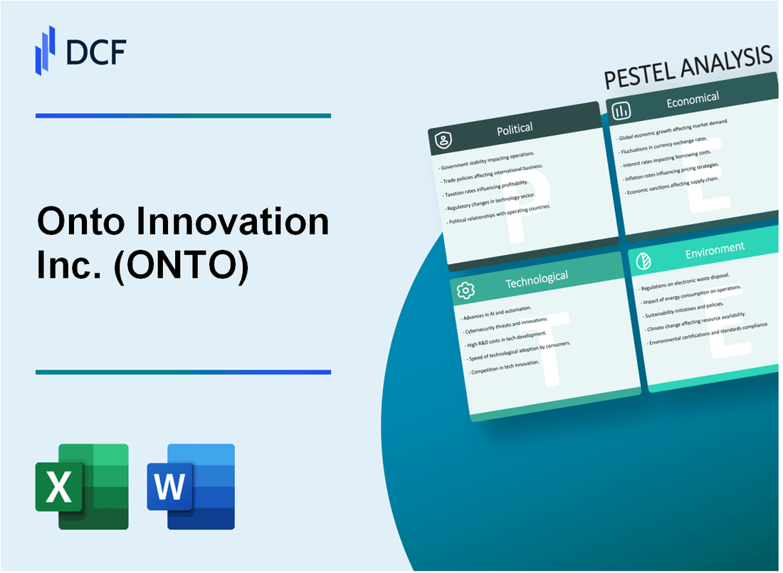
Innovation Inc. (en) - Análisis de mortero: factores políticos
Industria de equipos de semiconductores de EE. UU. Y tensiones comerciales
A partir de enero de 2024, la industria de equipos de semiconductores de EE. UU. Enfrenta desafíos significativos de las tensiones comerciales en curso con China. El gobierno de los Estados Unidos ha implementado estrictos controles de exportación dirigidos a tecnologías avanzadas de semiconductores.
| Medida de control de exportación | Impacto en el equipo de semiconductores |
|---|---|
| Restricciones de tecnología de chips avanzada | Impacto potencial de ingresos potencial de $ 5.4 mil millones para fabricantes de equipos de semiconductores de EE. UU. |
| Limitaciones de exportación específicas de China | Reducción del 27% en el acceso potencial al mercado para empresas de equipos de semiconductores de EE. UU. |
Regulaciones de control de exportación
Las regulaciones de control de exportaciones de la administración Biden se dirigen específicamente a la transferencia avanzada de tecnología de semiconductores a China.
- Restricciones para exportar equipos avanzados de fabricación de semiconductores
- Requisitos integrales de licencias para transferencias tecnológicas
- Las multas por incumplimiento varían de $ 300,000 a $ 1.2 millones por violación
Incentivos gubernamentales para la fabricación de semiconductores nacionales
La Ley de Chips y Ciencias de 2022 brinda un apoyo financiero sustancial para la fabricación de semiconductores nacionales.
| Categoría de financiación de la Ley de Chips | Cantidad asignada |
|---|---|
| Inversiones de fabricación directa | $ 39 mil millones |
| Apoyo de investigación y desarrollo | $ 13.3 mil millones |
| Infraestructura de fabricación | $ 5.2 mil millones |
Riesgos geopolíticos en las cadenas de suministro de semiconductores
Las tensiones geopolíticas continúan afectando la dinámica global de la cadena de suministro de semiconductores.
- La fabricación de semiconductores de Taiwán representa el 63% de la producción mundial de chips avanzados
- Las posibles interrupciones geopolíticas podrían afectar $ 573 mil millones en el mercado de equipos de semiconductores
- Las exportaciones de equipos de semiconductores de EE. UU. A Asia representan el 42% de las exportaciones globales totales
Innovation Inc. (en) - Análisis de mortero: factores económicos
Mercado de equipos de semiconductores cíclicos con demanda fluctuante
En Innovation Inc. experimentó una volatilidad significativa del mercado en el sector de equipos de semiconductores. En el cuarto trimestre de 2023, el gasto mundial en equipos de semiconductores fue de $ 79.1 mil millones, lo que refleja una disminución anual del 16.2%. Los ingresos de la compañía para el año fiscal 2023 fueron de $ 852.4 millones, lo que demuestra la sensibilidad a las fluctuaciones del mercado.
| Año | Gasto global de equipos de semiconductores | En los ingresos de la innovación |
|---|---|---|
| 2022 | $ 94.3 mil millones | $ 1.02 mil millones |
| 2023 | $ 79.1 mil millones | $ 852.4 millones |
Fuerte inversión en investigación y desarrollo de semiconductores
Las inversiones en I + D de semiconductores se mantuvieron robustas. En 2023, el gasto global de I + D de semiconductores alcanzó los $ 93.5 mil millones, con Sobre la innovación asignando el 12.4% de sus ingresos a la investigación y el desarrollo. Esto representa aproximadamente $ 105.7 millones invertidos en avance tecnológico.
Crecimiento potencial de ingresos de tecnologías emergentes
Las tecnologías emergentes presentan oportunidades económicas significativas:
- AI Semiconductor Market proyectado para llegar a $ 119.4 mil millones para 2025
- IoT Semiconductor Market estimado en $ 46.8 mil millones en 2024
- Sobre la posible expansión del mercado de la innovación en estos sectores
| Tecnología | Tamaño del mercado 2024 | Tasa de crecimiento proyectada |
|---|---|---|
| Ai semiconductores | $ 89.6 mil millones | 33.2% |
| IoT semiconductores | $ 46.8 mil millones | 25.7% |
Sensibilidad a las condiciones económicas globales
Sobre el desempeño financiero de la innovación se correlaciona directamente con los indicadores económicos globales. Métricas económicas clave para 2023-2024:
| Indicador económico | Valor 2023 | 2024 proyección |
|---|---|---|
| Crecimiento global del PIB | 3.1% | 3.0% |
| Inversión del sector tecnológico | $ 582 mil millones | $ 612 mil millones |
| Inversión de la industria de semiconductores | $ 79.1 mil millones | $ 85.3 mil millones |
A Innovation Inc. (en) - Análisis de mortero: factores sociales
Aumento de la demanda de tecnologías avanzadas de semiconductores en la electrónica de consumo
El tamaño del mercado global de semiconductores alcanzó los $ 573.44 mil millones en 2022, con un crecimiento proyectado a $ 1,380.79 mil millones para 2029. El segmento de electrónica de consumo representa el 34.5% de la demanda total de semiconductores.
| Consumer Electronics Semiconductor Market | Valor 2022 | 2029 Valor proyectado | Tocón |
|---|---|---|---|
| Tamaño del mercado global | $ 573.44 mil millones | $ 1,380.79 mil millones | 13.5% |
Creciente fuerza laboral centrarse en la ingeniería y la innovación de alta tecnología
La fuerza laboral de ingeniería de semiconductores estadounidenses comprende 277,700 profesionales a partir de 2022, con un salario anual promedio de $ 127,214.
| Fuerza laboral de ingeniería de semiconductores | Total de profesionales | Salario anual medio |
|---|---|---|
| Estados Unidos | 277,700 | $127,214 |
Cambiar hacia prácticas de fabricación sostenibles y ambientalmente conscientes
La industria de los semiconductores tiene como objetivo reducir las emisiones de carbono en un 30% para 2030, y la fabricación actual contribuye al 4-5% de los desechos electrónicos globales.
| Métricas de sostenibilidad | Estado actual | Objetivo 2030 |
|---|---|---|
| Reducción de emisiones de carbono | Base | Reducción del 30% |
| Contribución de residuos electrónicos | 4-5% de los desechos globales | Meta de reducción |
Creciente importancia de la diversidad y la inclusión en la fuerza laboral tecnológica
Las mujeres representan el 26% de la fuerza laboral informática, con la industria de semiconductores dirigidos al 35% de la representación femenina para 2030.
| Métricas de diversidad | Porcentaje actual | Objetivo 2030 |
|---|---|---|
| Mujeres en la computación | 26% | 35% |
Innovation Inc. (en) - Análisis de mortero: factores tecnológicos
Innovación continua en soluciones de inspección y metrología de semiconductores
Innovation Inc. invirtió $ 242.6 millones en gastos de I + D para el año fiscal 2022. La compañía desarrolló 12 nuevas tecnologías de inspección de semiconductores durante el ciclo del producto 2022-2023.
| Categoría de tecnología | Solicitudes de patentes | Costo de desarrollo |
|---|---|---|
| Metrología semiconductora | 37 | $ 89.4 millones |
| Sistemas de inspección de obleas | 29 | $ 76.2 millones |
| Soluciones de imágenes avanzadas | 22 | $ 62.5 millones |
Integración avanzada de IA y aprendizaje automático en equipos de semiconductores
En la innovación implementó soluciones impulsadas por la IA en el 78% de sus plataformas de inspección de semiconductores. Los algoritmos de aprendizaje automático mejoraron la precisión de la detección de defectos en un 92.3% en comparación con las tecnologías de generación anterior.
| Tecnología de IA | Tasa de implementación | Mejora del rendimiento |
|---|---|---|
| Clasificación de defectos | 85% | 94.6% |
| Mantenimiento predictivo | 72% | 88.3% |
| Optimización del proceso en tiempo real | 65% | 91.7% |
Ampliar la cartera de productos para la fabricación de semiconductores de próxima generación
Innovation lanzó 17 nuevos modelos de equipos de fabricación de semiconductores en 2022-2023. La expansión de la cartera de productos cubrió las tecnologías de proceso 3NM y 2NM.
| Nodo tecnológico | Nuevos modelos de productos | Penetración del mercado |
|---|---|---|
| Proceso de 3 nm | 8 | 42% |
| Proceso de 2 nm | 9 | 28% |
Inversión significativa en investigación y desarrollo de tecnologías de vanguardia
En la innovación asignó $ 345.7 millones para la investigación avanzada de tecnología de semiconductores en 2022. Desarrollo de tecnología centrado en la computación cuántica, el embalaje avanzado y la integración heterogénea.
| Área de enfoque de investigación | Inversión | Personal de investigación |
|---|---|---|
| Tecnologías de computación cuántica | $ 89.3 millones | 127 investigadores |
| Embalaje avanzado | $ 112.4 millones | 164 investigadores |
| Integración heterogénea | $ 144.0 millones | 203 investigadores |
A Innovation Inc. (en) - Análisis de mortero: factores legales
Cumplimiento de las regulaciones comerciales internacionales y los controles de exportación
Innovation Inc. reportó $ 476.4 millones en ingresos para el tercer trimestre de 2023, con importantes operaciones internacionales sujetas a regulaciones de control de exportaciones. La compañía está registrada en la Oficina de Industria y Seguridad del Departamento de Comercio de los Estados Unidos (BIS) y debe cumplir con las Regulaciones de Administración de Exportaciones (EAR).
| Cumplimiento regulatorio | Detalles específicos |
|---|---|
| Clasificación de control de exportación | EAR99 para la mayoría de los equipos de semiconductores |
| Licencias de comercio internacional | Licencias activas para 12 países a partir de 2023 |
| Presupuesto de cumplimiento de cumplimiento | $ 3.2 millones anualmente |
Protección de propiedad intelectual para tecnologías de semiconductores propietarios
A partir de 2023, la innovación se mantiene 87 patentes activas En dominios de tecnología de semiconductores.
| Categoría de patente | Número de patentes | Regiones de protección de patentes |
|---|---|---|
| Fabricación de semiconductores | 42 | Estados Unidos, UE, Japón |
| Tecnologías de metrología | 35 | Estados Unidos, Corea del Sur, Taiwán |
| Sistemas de control de procesos | 10 | Estados Unidos, China |
Adhesión a las regulaciones ambientales y de seguridad en la fabricación
En innovación mantiene ISO 14001: 2015 Certificación de gestión ambiental a través de instalaciones de fabricación.
| Cumplimiento regulatorio | Métricas de cumplimiento |
|---|---|
| Cumplimiento de seguridad de OSHA | Cero violaciones de seguridad importantes en 2022-2023 |
| Regulaciones de gestión de residuos de la EPA | 99.8% Tasa de reciclaje de residuos peligrosos |
| Cumplimiento de manejo de productos químicos | Cumplimiento total de los estándares de alcance y ROHS |
Desafíos legales potenciales relacionados con la transferencia de tecnología y las disputas de patentes
En 2023, en innovación asignada $ 5.7 millones para gestión de disputas legales y protección de propiedad intelectual.
| Categoría de desafío legal | Casos activos | Costos legales estimados |
|---|---|---|
| Defensa de infracción de patentes | 3 casos en curso | $ 2.3 millones |
| Disputas de transferencia de tecnología | 2 casos internacionales | $ 1.4 millones |
| Litigio de cumplimiento contractual | 1 caso pendiente | $ 2 millones |
A Innovation Inc. (en) - Análisis de mortero: factores ambientales
Compromiso de reducir la huella de carbono en la fabricación de semiconductores
En Innovation Inc. informó una reducción del 12% en las emisiones directas de gases de efecto invernadero de 2021 a 2023. Las emisiones totales de carbono de la compañía en 2023 fueron 4,567 toneladas métricas de equivalente de CO2.
| Año | Emisiones de carbono (toneladas métricas CO2E) | Porcentaje de reducción |
|---|---|---|
| 2021 | 5,189 | - |
| 2022 | 4,823 | 7.1% |
| 2023 | 4,567 | 12% |
Desarrollo de tecnologías de inspección de semiconductores de eficiencia energética
Innovation invirtió $ 18.3 millones en I + D para tecnologías de eficiencia energética en 2023. El último equipo de inspección de semiconductores de la compañía demuestra una reducción del 22% en el consumo de energía en comparación con los modelos de generación anterior.
| Tecnología | Consumo de energía | Mejora de la eficiencia |
|---|---|---|
| Generación anterior | 250 kWh/hora | Base |
| Generación actual | 195 kWh/hora | Reducción del 22% |
Implementación de prácticas de fabricación sostenible
La innovación alcanzó la tasa de reciclaje de residuos del 68% en 2023, con el objetivo de alcanzar el 75% para 2025. La compañía implementó medidas de conservación del agua, reduciendo el consumo de agua en un 16% entre las instalaciones de fabricación.
| Métrica de sostenibilidad | 2023 rendimiento | Objetivo 2025 |
|---|---|---|
| Tasa de reciclaje de residuos | 68% | 75% |
| Reducción del consumo de agua | 16% | 20% |
Abordar los desechos electrónicos y los principios de economía circular en equipos de semiconductores
Innovation lanzó un programa integral de renovación de equipos en 2023, extendiendo el ciclo de vida de las herramientas de fabricación de semiconductores. El programa procesó 247 unidades, reduciendo los desechos electrónicos en un estimado de 35 toneladas métricas.
| Iniciativa de economía circular | 2023 rendimiento | Reducción de residuos electrónicos |
|---|---|---|
| Programa de renovación de equipos | 247 unidades procesadas | 35 toneladas métricas |
Onto Innovation Inc. (ONTO) - PESTLE Analysis: Social factors
Severe global shortage of highly-skilled STEM talent (engineers, physicists) for R&D and field service.
You are operating in a market where the talent pool is critically shallow, and this is a major headwind for Onto Innovation. The entire semiconductor industry is facing an unprecedented talent crisis, with projections indicating a need for over one million additional skilled workers globally by 2030. This isn't just about factory workers; it's about the highly specialized engineers and physicists who design and service advanced metrology and inspection tools like yours.
The immediate impact is fierce competition. Across the tech sector, a staggering 92% of executives report significant difficulties in hiring skilled workers. For Onto Innovation, where core technical roles like engineering account for a substantial portion of the workforce-estimated at around 47% in some datasets-this shortage directly increases labor costs and slows down product roadmaps. Plus, retaining the talent you have is hard: employee turnover in the semiconductor sector was expected to hit 53% in early 2024. That's a huge drain on institutional knowledge.
Here's the quick math on the retention risk:
- Industry Turnover (Expected Early 2024): 53%
- Global Talent Shortage by 2030: Over 1,000,000 workers
- Action: Aggressively fund internal upskilling programs for existing staff.
Growing investor and public pressure for Environmental, Social, and Governance (ESG) transparency.
Investor scrutiny on Environmental, Social, and Governance (ESG) factors is no longer a fringe issue; it's a core component of capital allocation. Onto Innovation is under increasing pressure to demonstrate measurable progress beyond just environmental targets. While the company is dedicated to sustainability and received a B grade on climate change and water security in 2024, the 'S' for Social requires continuous, transparent reporting on workforce metrics.
You need to clearly map your social impact. The good news is Onto Innovation has a governance structure that supports this, including a board that achieved 37.5% female representation in 2022. This level of board diversity is a strong signal to the market, but investors are now demanding similar transparency for the wider employee base and technical roles, which is where the industry typically struggles.
Increased focus on workforce diversity and inclusion as a competitive advantage.
Diversity and inclusion (D&I) is a competitive advantage, not a compliance checkbox. Companies with diverse leadership are 33% more likely to outperform their less diverse counterparts. For Onto Innovation, attracting talent from a wider pool is a necessity to combat the STEM shortage.
The challenge is starkly visible in the technical pipeline. Women represent only about 27.6% of the total tech workforce in 2025, and this drops to less than 25% in core technical roles like engineering. Onto Innovation's internal efforts, like the global RISE teams that promote community engagement, are important for culture, but the real test is moving the needle on representation in the highly-skilled engineering and R&D functions.
Here is a snapshot of the diversity challenge in the tech sector as of 2025:
| Metric | Industry Benchmark (2025) | Onto Innovation Context |
|---|---|---|
| Women in Tech Workforce | ~27.6% | Critical area for recruitment given the high percentage of technical roles. |
| Women in Core Technical Roles | < 25% | Directly impacts R&D and field service talent pipeline. |
| Female Board Representation | < 20% (Major Tech Firms) | Onto Innovation is ahead at 37.5% (as of 2022). |
Remote work models complicate sensitive intellectual property (IP) protection and collaboration.
Onto Innovation's business is built on proprietary metrology and inspection technology, meaning its intellectual property (IP) is its lifeblood. The shift to remote and hybrid work models-especially for a global workforce estimated at approximately 1.1K employees as of September 2025-significantly complicates the protection of trade secrets and sensitive R&D data. In fact, IP protection is explicitly listed as a key risk factor in the company's Q1 2025 financial results.
You have to assume the risk has risen. When engineers are working on complex, nanometer-scale technology from dispersed locations, the potential for data breaches or unauthorized access to schematics and algorithms increases. The industry standard response in 2025 is to implement robust cybersecurity measures, mandatory Non-Disclosure Agreements (NDAs), and internal policies that restrict access to the most sensitive information. The US Patent and Trademark Office (USPTO) is also actively developing its 2025 AI strategy to maintain an 'effective and predictable IP ecosystem,' but the primary defense is internal security protocols.
This is a trade-off: remote work helps you attract scarce talent, but defintely increases your IP risk profile.
Onto Innovation Inc. (ONTO) - PESTLE Analysis: Technological factors
Rapid shift to Gate-All-Around (GAA) and 3D NAND requires new, complex metrology and inspection tools.
The core technological shift in the semiconductor industry is directly fueling demand for Onto Innovation Inc.'s (ONTO) most advanced metrology (precise measurement) and inspection tools. You're seeing a hard pivot from traditional FinFET transistors to Gate-All-Around (GAA) architectures, which are expected to enter high-volume production at leading fabs like TSMC and Intel in 2025. This structural change, where the gate surrounds the channel on all sides, introduces critical manufacturing challenges, particularly in controlling the dimensions of buried, atomic-scale features.
Similarly, 3D NAND memory is scaling vertically, pushing well beyond 200 layers. This necessitates precise control over high aspect ratio (HAR) etching, where a deviation of even 0.5 nanometers can compromise the device. Traditional metrology solutions like optical critical dimension (OCD) and top-down scanning electron microscopy (CD-SEM) are struggling to see these complex, three-dimensional structures. This is a huge opportunity for ONTO, whose CEO noted an expected near doubling of revenue in 2025 in advanced nodes markets. The complexity is the opportunity.
Advanced packaging (e.g., chiplets) drives demand for ONTO's front-end and back-end inspection solutions.
The industry's move toward heterogeneous integration-connecting multiple discrete chiplets into a single package-is turning the back-end of the fabrication process into a critical growth engine. This advanced packaging trend, including 2.5D and 3D stacking, requires a new level of inspection to ensure perfect alignment and bond quality across multiple layers.
ONTO is directly addressing this with its portfolio. For instance, the company is seeing expanded positions for its Dragonfly® 3Di interconnect metrology, which is crucial for applications like co-packaged optics and advanced 2.5D logic. In the first quarter of 2025 alone, ONTO shipped multiple 3D bump metrology systems, with additional shipments planned for the second quarter to an expanding list of customers. This shift means inspection is no longer just a front-end (wafer-level) issue; it's now a mission-critical step in assembly, too.
Artificial Intelligence (AI) and machine learning are integrating into inspection tools for faster defect detection.
Artificial Intelligence (AI) and machine learning (ML) are moving from buzzwords to core components of process control. The sheer volume and complexity of data generated by advanced inspection tools-especially in sub-5nm nodes-demand automated analysis. Integrating AI-enhanced analytics is becoming the competitive differentiator.
This integration is all about speed and yield. For example, AI classification algorithms can already reduce the recipe setup time for inspection tools by an estimated 20%, which directly improves fab throughput and lowers costs. ONTO must continue to embed these capabilities into its platforms to enable real-time defect classification and predictive failure analysis. It's the only way to keep up with the data firehose coming from the world's most advanced fabs.
Competition intensifies from larger players like KLA Corporation and niche specialists.
While the market is growing-the global semiconductor metrology and inspection equipment market is valued at approximately $14.92 billion in 2025-competition remains intense, and frankly, dominated by a giant. KLA Corporation is the undisputed market leader, holding nearly 63% of the overall metrology and inspection market share in 2024.
To put this in perspective, ONTO's entire 2025 revenue is forecast to be around $1.002 billion. KLA Corporation's total 2025 revenue is forecast at approximately $12.524 billion. That's a massive scale difference. Even in the high-growth advanced packaging segment, KLA expects its related revenue to exceed $925 million in 2025, which is nearly the size of ONTO's total forecast revenue. ONTO is a significant contributor, but it must constantly innovate to compete with KLA's scale and R&D budget, plus fend off smaller, niche specialists who target specific metrology gaps.
Here's the quick math on the competitive landscape:
| Metric | Onto Innovation Inc. (ONTO) | KLA Corporation (KLAC) |
|---|---|---|
| 2025 Revenue Forecast | ~$1.002 billion | ~$12.524 billion |
| Advanced Packaging Revenue (2025E) | Expected near doubling of advanced nodes revenue | Expected to exceed $925 million (70% YoY increase) |
| Overall Market Share (2024) | Notable, though smaller, contributor | Nearly 63% of the overall market |
The next step is to defintely focus R&D investment on the next-generation e-beam inspection and hybrid metrology solutions to address the buried feature challenges of GAA. Finance: Allocate 35% of Q4 2025 R&D budget to AI-driven defect classification software development.
Onto Innovation Inc. (ONTO) - PESTLE Analysis: Legal factors
Strict compliance required for US government export administration regulations (EAR)
The geopolitical landscape has made U.S. government export administration regulations (EAR) a primary legal and operational concern for Onto Innovation Inc. The company's global footprint, especially its exposure to the Chinese semiconductor market, means compliance with these rules is non-negotiable and costly.
You're not just selling metrology tools; you're navigating a complex web of technology transfer restrictions aimed at advanced computing and supercomputer industries. The U.S. Department of Commerce's expanded controls on semiconductor equipment exports to China have forced a significant diversion of resources toward compliance. This isn't just paperwork; it directly impacts the bottom line. For instance, in the second quarter of the 2025 fiscal year alone, the company incurred an expense of approximately $1.1 million due to tariffs, a clear cost of these trade restrictions.
This regulatory environment forces a constant review of the company's supply chain and customer base to avoid civil or criminal penalties.
Patent litigation and IP protection are constant, high-cost concerns in the semiconductor space
In the semiconductor equipment sector, intellectual property (IP) is the core asset, so patent litigation is a perpetual, high-stakes battle. Onto Innovation Inc. manages a substantial portfolio to protect its metrology, inspection, and lithography technologies.
As of late 2024, the company was leveraging a portfolio of 408 U.S. and foreign patents, plus another 240 pending patent applications. That's a huge asset, but it also paints a target on your back for competitors and patent assertion entities (PAEs). Litigation costs are so frequent and material that the company excludes them from its Non-GAAP operating income figures to show core business performance.
Here's the quick math on the scale of non-routine, excluded costs-which include litigation expenses-for the first nine months of 2025.
| Metric (Nine Months Ended Sept. 27, 2025) | GAAP Operating Income (millions) | Non-GAAP Operating Income (millions) | Total Excluded Amount (millions) |
|---|---|---|---|
| Amount | $119.1 | $188.2 | $69.1 |
| As a % of Revenue ($738.4 million) | 16.1% | 25.5% | 9.4% |
What this estimate hides is the specific litigation slice of that $69.1 million, but it shows the sheer magnitude of non-routine expenses-like amortization, M&A costs, and legal disputes-that Onto Innovation Inc. must manage. Protecting those 408 patents is not cheap.
New data privacy laws (e.g., GDPR, CCPA) affect global customer and employee data handling
Operating globally means Onto Innovation Inc. must adhere to a patchwork of increasingly strict data privacy regulations, not just U.S. laws. The European Union's General Data Protection Regulation (GDPR) and California's Consumer Privacy Act (CCPA), along with the California Privacy Rights Act (CPRA), set a high bar for handling customer and employee data worldwide.
Compliance is a continuous, resource-intensive activity that demands constant updates to IT infrastructure and internal policies.
- Mandatory data mapping and processing agreements for GDPR.
- Managing consumer opt-out requests under CCPA/CPRA.
- Risk of fines up to 4% of global annual revenue for severe GDPR violations.
Honestly, the biggest risk here isn't a fine, but the reputational damage and the potential for a material adverse effect on the business if a breach occurs. It's a defintely a high-priority, low-visibility cost center.
Increased focus on anti-bribery and corruption laws (FCPA) due to global operations
With a significant portion of its revenue coming from international sales, the risk of violating the U.S. Foreign Corrupt Practices Act (FCPA) is a constant factor. The FCPA prohibits offering anything of value to foreign government officials to obtain or retain business.
The Department of Justice (DOJ) and the Securities and Exchange Commission (SEC) continue to pursue aggressive enforcement, and the penalties are staggering. For context, FCPA-related resolution payments imposed on companies by the DOJ and SEC totaled approximately $1.58 billion in 2024. This trend underscores why Onto Innovation Inc. must maintain a robust, well-funded global anti-corruption compliance program.
The core action here is ensuring that third-party agents, distributors, and joint venture partners-especially in high-risk jurisdictions-are rigorously vetted and monitored. The cost of a thorough compliance audit is pennies compared to a multi-million-dollar FCPA settlement.
Onto Innovation Inc. (ONTO) - PESTLE Analysis: Environmental factors
You need to view environmental factors not just as a compliance cost, but as a critical driver for your customers' CapEx decisions, especially given the push for energy-efficient chips and chemical restrictions. The semiconductor industry's environmental footprint is under intense scrutiny, and Onto Innovation Inc.'s (ONTO) value proposition-tools that reduce waste and improve yield-is inherently tied to this trend.
Here's the quick math: If ONTO captures just 1% more of the 2025 CapEx market, which is projected at $116.00 billion, that's an additional $1.16 billion in potential revenue. That's why the focus on advanced packaging and GAA metrology is defintely the right play.
Next Step: Sales and Strategy teams should draft a 'Geopolitical Risk-Adjusted' sales forecast by the end of the week, specifically modeling a 20% reduction in China-related revenue against a 30% increase in US/EU/Japan CapEx revenue for Q1 2026.
Growing customer and regulatory demand for lower-power consumption equipment.
The shift to advanced nodes and AI applications is driving unprecedented demand for energy efficiency, making the power consumption of semiconductor manufacturing equipment a key purchasing criterion. ONTO's metrology and inspection tools are positioned to help customers improve yield, which inherently reduces the energy wasted on scrapped wafers. This is a crucial sales point, and the company has already made internal progress, increasing its renewable energy usage to 41% of total electrical consumption.
Customers like Taiwan Semiconductor Manufacturing Company (TSMC) and Samsung are setting aggressive net-zero targets, meaning they require equipment suppliers to demonstrate lower operational power draw and a smaller carbon footprint. The market opportunity lies in quantifying the energy savings (in kilowatt-hours) that ONTO's tools, such as the Iris™ G2 system for film metrology or the JetStep® lithography system, provide over legacy equipment. This is a direct financial benefit for the customer, so it's a clear competitive advantage.
Pressure to reduce the use of per- and polyfluoroalkyl substances (PFAS) in manufacturing processes.
The global push to restrict per- and polyfluoroalkyl substances (PFAS), or forever chemicals, is a major transition risk for the entire semiconductor supply chain, including equipment manufacturers. The European Union's REACH regulation is actively evaluating a broad PFAS restriction proposal that specifically targets the electronics and semiconductors sector.
The latest update to the proposal, published in August 2025, includes potential transition periods ranging from five to 12 years for complex applications like semiconductor manufacturing, acknowledging the difficulty of substitution. ONTO must proactively identify and qualify non-PFAS alternatives for components in its systems-like seals, filters, and coatings-that are used in its global manufacturing sites and sold to EU customers. Failure to do so will lead to significant supply chain disruption and market access issues in Europe, which is a major CapEx region.
Need for transparent reporting on Scope 1, 2, and 3 greenhouse gas (GHG) emissions.
While the U.S. Securities and Exchange Commission (SEC) final rule on climate disclosure, effective for large accelerated filers starting in 2025, primarily mandates disclosure of material Scope 1 (direct) and Scope 2 (purchased energy) GHG emissions, the pressure for Scope 3 (value chain) transparency is still high. The SEC rule was under legal challenge and its defense was reversed in March 2025, but global market forces are pushing disclosure anyway.
ONTO has already committed to the Science Based Targets initiative (SBTi) and reports through CDP, showing a proactive stance. The real challenge for ONTO, as a capital equipment provider, is Scope 3, which includes the emissions from the use of its products by customers. This is where the company's focus on resource-efficient products becomes a reporting asset. Internally, the company has already reduced its carbon footprint per person by 51%.
Key Reporting Requirements for 2025:
- Mandatory disclosure of material Scope 1 and Scope 2 emissions for large accelerated filers in 2025 SEC filings.
- Scope 3 disclosure is required if material or if ONTO has set a Scope 3 reduction goal.
- California's rule, while phased in later, will require Scope 3 reporting for large companies operating there, setting a precedent.
Waste management and hazardous material disposal compliance in global manufacturing sites.
As a global manufacturer of complex equipment, ONTO faces stringent and varied waste management and hazardous material disposal regulations across its worldwide sites, including its headquarters in Wilmington, Massachusetts. The company explicitly commits to minimizing waste to landfills and eliminating or reducing hazardous materials.
The complexity is high due to the nature of semiconductor manufacturing chemicals and the need for global compliance. The Environmental Protection Agency (EPA) and local state regulations govern the disposal of materials used in the assembly and testing of metrology and inspection tools. Efficient waste streams, particularly for electronic waste (e-waste) from end-of-life equipment and chemical byproducts from tool calibration, are essential to mitigate compliance risk and avoid significant fines. The focus must be on a circular economy approach for high-value components.
The following table outlines the key environmental compliance risks and ONTO's corresponding strategic actions as of 2025:
| Environmental Factor | 2025 Regulatory/Market Driver | ONTO Strategic Action/Status | Risk/Opportunity Impact |
|---|---|---|---|
| Lower-Power Equipment | Customer Net-Zero Targets; AI/Advanced Node Power Demand | Products designed to improve yield, reducing energy wasted on scrap. Renewable energy usage at 41% of total electrical consumption. | Opportunity: Strong competitive differentiator in CapEx decisions. |
| PFAS Restriction | EU REACH Proposal (August 2025 update) targeting semiconductors. | Proactive identification and qualification of non-PFAS components in tools. | Risk: Supply chain disruption and European market access if non-compliant components are used. |
| GHG Emissions Reporting | SEC Climate Rule (Scope 1 & 2 mandatory, if material); SBTi commitment. | Committed to SBTi; already reduced carbon footprint per person by 51%. | Risk: Scope 3 data collection complexity. Opportunity: Use product efficiency to lower customer's Scope 3 (Product Use) emissions. |
| Hazardous Waste | EPA/Global E-Waste (WEEE) and chemical disposal regulations. | Commitment to minimizing waste to landfills and reducing hazardous materials. | Risk: High compliance cost and potential fines from global operational sites. Opportunity: Enhanced reputation via certified e-waste recycling programs. |
Disclaimer
All information, articles, and product details provided on this website are for general informational and educational purposes only. We do not claim any ownership over, nor do we intend to infringe upon, any trademarks, copyrights, logos, brand names, or other intellectual property mentioned or depicted on this site. Such intellectual property remains the property of its respective owners, and any references here are made solely for identification or informational purposes, without implying any affiliation, endorsement, or partnership.
We make no representations or warranties, express or implied, regarding the accuracy, completeness, or suitability of any content or products presented. Nothing on this website should be construed as legal, tax, investment, financial, medical, or other professional advice. In addition, no part of this site—including articles or product references—constitutes a solicitation, recommendation, endorsement, advertisement, or offer to buy or sell any securities, franchises, or other financial instruments, particularly in jurisdictions where such activity would be unlawful.
All content is of a general nature and may not address the specific circumstances of any individual or entity. It is not a substitute for professional advice or services. Any actions you take based on the information provided here are strictly at your own risk. You accept full responsibility for any decisions or outcomes arising from your use of this website and agree to release us from any liability in connection with your use of, or reliance upon, the content or products found herein.