
|
Sur Innovation Inc. (sur): Analyse du Pestle [Jan-2025 Mise à jour] |
Entièrement Modifiable: Adapté À Vos Besoins Dans Excel Ou Sheets
Conception Professionnelle: Modèles Fiables Et Conformes Aux Normes Du Secteur
Pré-Construits Pour Une Utilisation Rapide Et Efficace
Compatible MAC/PC, entièrement débloqué
Aucune Expertise N'Est Requise; Facile À Suivre
Onto Innovation Inc. (ONTO) Bundle
Dans le monde dynamique de la technologie des semi-conducteurs, sur Innovation Inc. (sur) se dresse au carrefour de la transformation technologique mondiale, naviguant dans un paysage complexe de tensions politiques, de volatilité économique et de progrès technologique rapide. Alors que l'industrie des semi-conducteurs devient de plus en plus essentielle à l'innovation mondiale, cette analyse de pilon dévoile les défis et les opportunités à multiples facettes qui façonnent le positionnement stratégique dans un écosystème technologique en évolution rapide. De la dynamique du commerce géopolitique à l'intégration de l'IA de pointe, le parcours de l'entreprise reflète l'interaction complexe des facteurs qui définissent la fabrication et l'innovation de haute technologie modernes.
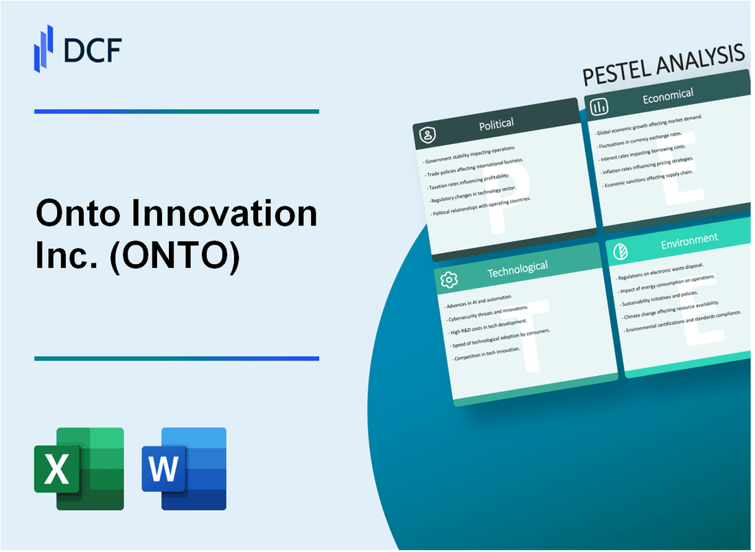
Sur Innovation Inc. (sur) - Analyse du pilon: facteurs politiques
Industrie américaine des équipements semi-conducteurs et tensions commerciales
En janvier 2024, l'industrie américaine des équipements de semi-conducteurs est confrontée à des défis importants des tensions commerciales en cours avec la Chine. Le gouvernement américain a mis en œuvre des contrôles d'exportation stricts ciblant les technologies avancées des semi-conducteurs.
| Mesure de contrôle des exportations | Impact sur l'équipement semi-conducteur |
|---|---|
| Restrictions de technologie des puces avancées | 5,4 milliards de dollars à l'impact des revenus potentiels pour les fabricants d'équipements de semi-conducteurs américains |
| Limitations d'exportation spécifiques à la Chine | Réduction de 27% de l'accès potentiel sur le marché pour les sociétés d'équipement semi-conducteur américain |
Règlement sur le contrôle des exportations
Les réglementations de contrôle des exportations de l'administration Biden ciblent spécifiquement le transfert de technologie avancée de semi-conducteurs avancés en Chine.
- Restrictions sur l'exportation d'équipements de fabrication avancés de semi-conducteurs
- Exigences complètes de licence pour les transferts technologiques
- Les pénalités de non-conformité varient de 300 000 $ à 1,2 million de dollars par violation
Incitations du gouvernement pour la fabrication de semi-conducteurs intérieurs
La Chips and Science Act de 2022 fournit un soutien financier substantiel à la fabrication intérieure des semi-conducteurs.
| Catégorie de financement de la loi sur les puces | Montant alloué |
|---|---|
| Investissements manufacturiers directs | 39 milliards de dollars |
| Support de recherche et développement | 13,3 milliards de dollars |
| Infrastructure de fabrication | 5,2 milliards de dollars |
Risques géopolitiques dans les chaînes d'approvisionnement des semi-conducteurs
Les tensions géopolitiques continuent d'avoir un impact sur la dynamique mondiale de la chaîne d'approvisionnement des semi-conducteurs.
- La fabrication de semi-conducteurs de Taiwan représente 63% de la production mondiale de puces avancées
- Les perturbations géopolitiques potentielles pourraient avoir un impact sur 573 milliards de dollars sur le marché des équipements semi-conducteurs
- Les exportations d'équipement semi-conducteur américain vers l'Asie représentent 42% du total des exportations mondiales
Sur Innovation Inc. (sur) - Analyse du pilon: facteurs économiques
Marché des équipements à semi-conducteurs cycliques avec une demande fluctuante
Sur Innovation Inc. a connu une volatilité significative du marché dans le secteur des équipements de semi-conducteurs. Au quatrième trimestre 2023, les dépenses mondiales d'équipement de semi-conducteur étaient de 79,1 milliards de dollars, reflétant une baisse de 16,2% en glissement annuel. Les revenus de la société pour l'exercice 2023 étaient de 852,4 millions de dollars, démontrant une sensibilité aux fluctuations du marché.
| Année | Dépenses mondiales d'équipement de semi-conducteur | Sur les revenus d'innovation |
|---|---|---|
| 2022 | 94,3 milliards de dollars | 1,02 milliard de dollars |
| 2023 | 79,1 milliards de dollars | 852,4 millions de dollars |
Investissement solide dans la recherche et le développement de semi-conducteurs
Les investissements en R&D semi-conducteurs sont restés robustes. En 2023, les dépenses mondiales de R&D semi-conducteurs ont atteint 93,5 milliards de dollars, avec Sur l'innovation allouant 12,4% de ses revenus à la recherche et au développement. Cela représente environ 105,7 millions de dollars investis dans les progrès technologiques.
Croissance potentielle des revenus des technologies émergentes
Les technologies émergentes présentent des opportunités économiques importantes:
- Le marché des semi-conducteurs d'IA prévoyait à 119,4 milliards de dollars d'ici 2025
- Marché des semi-conducteurs IoT estimé à 46,8 milliards de dollars en 2024
- Sur l'expansion potentielle du marché de l'innovation dans ces secteurs
| Technologie | 2024 Taille du marché | Taux de croissance projeté |
|---|---|---|
| Semi-conducteurs d'IA | 89,6 milliards de dollars | 33.2% |
| Semi-conducteurs IoT | 46,8 milliards de dollars | 25.7% |
Sensibilité aux conditions économiques mondiales
Sur la performance financière d'Innovation est directement en corrélation avec les indicateurs économiques mondiaux. Mesures économiques clés pour 2023-2024:
| Indicateur économique | Valeur 2023 | 2024 projection |
|---|---|---|
| Croissance mondiale du PIB | 3.1% | 3.0% |
| Investissement du secteur de la technologie | 582 milliards de dollars | 612 milliards de dollars |
| Investissement de l'industrie des semi-conducteurs | 79,1 milliards de dollars | 85,3 milliards de dollars |
Sur Innovation Inc. (sur) - Analyse du pilon: facteurs sociaux
Demande croissante de technologies avancées de semi-conducteurs dans l'électronique grand public
La taille du marché mondial des semi-conducteurs a atteint 573,44 milliards de dollars en 2022, avec une croissance projetée à 1 380,79 milliards de dollars d'ici 2029. Le segment de l'électronique grand public représente 34,5% de la demande totale de semi-conducteurs.
| Marché des semi-conducteurs à l'électronique grand public | Valeur 2022 | 2029 Valeur projetée | TCAC |
|---|---|---|---|
| Taille du marché mondial | 573,44 milliards de dollars | 1 380,79 milliards de dollars | 13.5% |
La main-d'œuvre croissante se concentre sur l'ingénierie et l'innovation de haute technologie
La main-d'œuvre d'ingénierie des semi-conducteurs américains comprend 277 700 professionnels en 2022, avec un salaire annuel médian de 127 214 $.
| Travail d'ingénierie des semi-conducteurs | Total des professionnels | Salaire annuel médian |
|---|---|---|
| États-Unis | 277,700 | $127,214 |
Vers les pratiques de fabrication durables et soucieuses de l'environnement
L'industrie des semi-conducteurs vise à réduire les émissions de carbone de 30% d'ici 2030, la fabrication actuelle contribuant à 4 à 5% des déchets électroniques mondiaux.
| Métriques de durabilité | État actuel | Cible 2030 |
|---|---|---|
| Réduction des émissions de carbone | Base de base | Réduction de 30% |
| Contribution des déchets électroniques | 4 à 5% des déchets mondiaux | Objectif de réduction |
Importance croissante de la diversité et de l'inclusion dans la technologie technologique
Les femmes représentent 26% de la main-d'œuvre informatique, l'industrie des semi-conducteurs ciblant 35% de représentation féminine d'ici 2030.
| Métriques de la diversité | Pourcentage actuel | Cible 2030 |
|---|---|---|
| Femmes en informatique | 26% | 35% |
Sur Innovation Inc. (sur) - Analyse du pilon: facteurs technologiques
Innovation continue dans les solutions d'inspection et de métrologie des semi-conducteurs
Sur Innovation Inc. a investi 242,6 millions de dollars dans les dépenses de R&D pour l'exercice 2022. La société a développé 12 nouvelles technologies d'inspection des semi-conducteurs au cours du cycle de produit 2022-2023.
| Catégorie de technologie | Demandes de brevet | Coût de développement |
|---|---|---|
| Métrologie des semi-conducteurs | 37 | 89,4 millions de dollars |
| Systèmes d'inspection des plaquettes | 29 | 76,2 millions de dollars |
| Solutions d'imagerie avancées | 22 | 62,5 millions de dollars |
Intégration avancée de l'IA et de l'apprentissage automatique dans l'équipement semi-conducteur
Sur l'innovation a mis en œuvre des solutions axées sur l'IA dans 78% de ses plateformes d'inspection de semi-conducteurs. Les algorithmes d'apprentissage automatique ont amélioré la précision de détection des défauts de 92,3% par rapport aux technologies de génération précédente.
| Technologie d'IA | Taux de mise en œuvre | Amélioration des performances |
|---|---|---|
| Classification des défauts | 85% | 94.6% |
| Maintenance prédictive | 72% | 88.3% |
| Optimisation de processus en temps réel | 65% | 91.7% |
Expansion du portefeuille de produits pour la fabrication de semi-conducteurs de nouvelle génération
Sur l'innovation a lancé 17 nouveaux modèles d'équipements de fabrication de semi-conducteurs en 2022-2023. L'expansion du portefeuille de produits a couvert les technologies de processus 3 nm et 2 nm.
| Nœud technologique | Nouveaux modèles de produits | Pénétration du marché |
|---|---|---|
| Processus 3NM | 8 | 42% |
| Processus 2NM | 9 | 28% |
Investissement important dans la recherche et le développement de technologies de pointe
Sur l'innovation, il a alloué 345,7 millions de dollars pour la recherche avancée en technologie des semi-conducteurs en 2022. Le développement de la technologie s'est concentré sur l'informatique quantique, l'emballage avancé et l'intégration hétérogène.
| Domaine de mise au point de recherche | Investissement | Personnel de recherche |
|---|---|---|
| Technologies informatiques quantiques | 89,3 millions de dollars | 127 chercheurs |
| Emballage avancé | 112,4 millions de dollars | 164 chercheurs |
| Intégration hétérogène | 144,0 millions de dollars | 203 chercheurs |
Sur Innovation Inc. (sur) - Analyse du pilon: facteurs juridiques
Conformité aux réglementations du commerce international et aux contrôles d'exportation
Sur Innovation Inc. a déclaré 476,4 millions de dollars de revenus pour le troisième trimestre 2023, avec des opérations internationales importantes sous réserve des réglementations de contrôle des exportations. La société est enregistrée auprès du Bureau de l'industrie et de la sécurité du Département américain du commerce (BIS) et doit se conformer aux réglementations sur l'administration des exportations (EAR).
| Conformité réglementaire | Détails spécifiques |
|---|---|
| Classification de contrôle des exportations | EAR99 pour la plupart des équipements semi-conducteurs |
| Licences commerciales internationales | Licences actives pour 12 pays à partir de 2023 |
| Budget d'application de la conformité | 3,2 millions de dollars par an |
Protection de la propriété intellectuelle pour les technologies propriétaires de semi-conducteurs
Depuis 2023, sur l'innovation titulaire 87 brevets actifs Dans les domaines technologiques des semi-conducteurs.
| Catégorie de brevet | Nombre de brevets | Régions de protection des brevets |
|---|---|---|
| Fabrication de semi-conducteurs | 42 | États-Unis, UE, Japon |
| Technologies de métrologie | 35 | États-Unis, Corée du Sud, Taïwan |
| Systèmes de contrôle des processus | 10 | États-Unis, Chine |
Adhésion aux réglementations environnementales et de sécurité dans la fabrication
Sur l'innovation maintient ISO 14001: Certification de gestion de l'environnement 2015 dans toutes les installations de fabrication.
| Conformité réglementaire | Métriques de conformité |
|---|---|
| Conformité de la sécurité de l'OSHA | Zéro violations de sécurité majeures en 2022-2023 |
| Règlements sur la gestion des déchets de l'EPA | Taux de recyclage des déchets à 99,8% |
| Compliance de la manipulation des produits chimiques | Compliance complète avec les normes de portée et de ROHS |
Défis juridiques potentiels liés au transfert de technologie et aux litiges de brevet
En 2023, sur l'innovation allouée 5,7 millions de dollars pour la gestion des différends juridiques et la protection de la propriété intellectuelle.
| Catégorie de défi juridique | Cas actifs | Frais juridiques estimés |
|---|---|---|
| Défense d'infraction aux brevets | 3 cas en cours | 2,3 millions de dollars |
| Conflits de transfert de technologie | 2 cas internationaux | 1,4 million de dollars |
| Litige de conformité contractuelle | 1 cas en attente | 2 millions de dollars |
Sur Innovation Inc. (sur) - Analyse du pilon: facteurs environnementaux
Engagement à réduire l'empreinte carbone dans la fabrication de semi-conducteurs
Sur Innovation Inc. a signalé une réduction de 12% des émissions directes de gaz à effet de serre de 2021 à 2023. Les émissions totales de carbone de la société en 2023 étaient de 4 567 tonnes métriques d'équivalent CO2.
| Année | Émissions de carbone (tonnes métriques CO2E) | Pourcentage de réduction |
|---|---|---|
| 2021 | 5,189 | - |
| 2022 | 4,823 | 7.1% |
| 2023 | 4,567 | 12% |
Développement de technologies d'inspection des semi-conducteurs éconergétiques
Sur Innovation a investi 18,3 millions de dollars dans la R&D pour les technologies économes en énergie en 2023. Le dernier équipement d'inspection des semi-conducteurs de la société démontre une réduction de 22% de la consommation d'énergie par rapport aux modèles de génération précédente.
| Technologie | Consommation d'énergie | Amélioration de l'efficacité |
|---|---|---|
| Génération précédente | 250 kWh / heure | Base de base |
| Génération actuelle | 195 kWh / heure | Réduction de 22% |
Mettre en œuvre des pratiques de fabrication durables
Sur l'innovation a atteint un taux de recyclage des déchets de 68% en 2023, dans le but d'atteindre 75% d'ici 2025. La société a mis en œuvre des mesures de conservation de l'eau, réduisant la consommation d'eau de 16% entre les installations de fabrication.
| Métrique de la durabilité | Performance de 2023 | Cible 2025 |
|---|---|---|
| Taux de recyclage des déchets | 68% | 75% |
| Réduction de la consommation d'eau | 16% | 20% |
Aborder les principes électroniques des déchets et de l'économie circulaire dans l'équipement semi-conducteur
Sur Innovation a lancé un programme complet de rénovation de l'équipement en 2023, prolongeant le cycle de vie des outils de fabrication de semi-conducteurs. Le programme a traité 247 unités, réduisant les déchets électroniques d'environ 35 tonnes métriques.
| Initiative de l'économie circulaire | Performance de 2023 | Réduction des déchets électroniques |
|---|---|---|
| Programme de rénovation de l'équipement | 247 unités traitées | 35 tonnes métriques |
Onto Innovation Inc. (ONTO) - PESTLE Analysis: Social factors
Severe global shortage of highly-skilled STEM talent (engineers, physicists) for R&D and field service.
You are operating in a market where the talent pool is critically shallow, and this is a major headwind for Onto Innovation. The entire semiconductor industry is facing an unprecedented talent crisis, with projections indicating a need for over one million additional skilled workers globally by 2030. This isn't just about factory workers; it's about the highly specialized engineers and physicists who design and service advanced metrology and inspection tools like yours.
The immediate impact is fierce competition. Across the tech sector, a staggering 92% of executives report significant difficulties in hiring skilled workers. For Onto Innovation, where core technical roles like engineering account for a substantial portion of the workforce-estimated at around 47% in some datasets-this shortage directly increases labor costs and slows down product roadmaps. Plus, retaining the talent you have is hard: employee turnover in the semiconductor sector was expected to hit 53% in early 2024. That's a huge drain on institutional knowledge.
Here's the quick math on the retention risk:
- Industry Turnover (Expected Early 2024): 53%
- Global Talent Shortage by 2030: Over 1,000,000 workers
- Action: Aggressively fund internal upskilling programs for existing staff.
Growing investor and public pressure for Environmental, Social, and Governance (ESG) transparency.
Investor scrutiny on Environmental, Social, and Governance (ESG) factors is no longer a fringe issue; it's a core component of capital allocation. Onto Innovation is under increasing pressure to demonstrate measurable progress beyond just environmental targets. While the company is dedicated to sustainability and received a B grade on climate change and water security in 2024, the 'S' for Social requires continuous, transparent reporting on workforce metrics.
You need to clearly map your social impact. The good news is Onto Innovation has a governance structure that supports this, including a board that achieved 37.5% female representation in 2022. This level of board diversity is a strong signal to the market, but investors are now demanding similar transparency for the wider employee base and technical roles, which is where the industry typically struggles.
Increased focus on workforce diversity and inclusion as a competitive advantage.
Diversity and inclusion (D&I) is a competitive advantage, not a compliance checkbox. Companies with diverse leadership are 33% more likely to outperform their less diverse counterparts. For Onto Innovation, attracting talent from a wider pool is a necessity to combat the STEM shortage.
The challenge is starkly visible in the technical pipeline. Women represent only about 27.6% of the total tech workforce in 2025, and this drops to less than 25% in core technical roles like engineering. Onto Innovation's internal efforts, like the global RISE teams that promote community engagement, are important for culture, but the real test is moving the needle on representation in the highly-skilled engineering and R&D functions.
Here is a snapshot of the diversity challenge in the tech sector as of 2025:
| Metric | Industry Benchmark (2025) | Onto Innovation Context |
|---|---|---|
| Women in Tech Workforce | ~27.6% | Critical area for recruitment given the high percentage of technical roles. |
| Women in Core Technical Roles | < 25% | Directly impacts R&D and field service talent pipeline. |
| Female Board Representation | < 20% (Major Tech Firms) | Onto Innovation is ahead at 37.5% (as of 2022). |
Remote work models complicate sensitive intellectual property (IP) protection and collaboration.
Onto Innovation's business is built on proprietary metrology and inspection technology, meaning its intellectual property (IP) is its lifeblood. The shift to remote and hybrid work models-especially for a global workforce estimated at approximately 1.1K employees as of September 2025-significantly complicates the protection of trade secrets and sensitive R&D data. In fact, IP protection is explicitly listed as a key risk factor in the company's Q1 2025 financial results.
You have to assume the risk has risen. When engineers are working on complex, nanometer-scale technology from dispersed locations, the potential for data breaches or unauthorized access to schematics and algorithms increases. The industry standard response in 2025 is to implement robust cybersecurity measures, mandatory Non-Disclosure Agreements (NDAs), and internal policies that restrict access to the most sensitive information. The US Patent and Trademark Office (USPTO) is also actively developing its 2025 AI strategy to maintain an 'effective and predictable IP ecosystem,' but the primary defense is internal security protocols.
This is a trade-off: remote work helps you attract scarce talent, but defintely increases your IP risk profile.
Onto Innovation Inc. (ONTO) - PESTLE Analysis: Technological factors
Rapid shift to Gate-All-Around (GAA) and 3D NAND requires new, complex metrology and inspection tools.
The core technological shift in the semiconductor industry is directly fueling demand for Onto Innovation Inc.'s (ONTO) most advanced metrology (precise measurement) and inspection tools. You're seeing a hard pivot from traditional FinFET transistors to Gate-All-Around (GAA) architectures, which are expected to enter high-volume production at leading fabs like TSMC and Intel in 2025. This structural change, where the gate surrounds the channel on all sides, introduces critical manufacturing challenges, particularly in controlling the dimensions of buried, atomic-scale features.
Similarly, 3D NAND memory is scaling vertically, pushing well beyond 200 layers. This necessitates precise control over high aspect ratio (HAR) etching, where a deviation of even 0.5 nanometers can compromise the device. Traditional metrology solutions like optical critical dimension (OCD) and top-down scanning electron microscopy (CD-SEM) are struggling to see these complex, three-dimensional structures. This is a huge opportunity for ONTO, whose CEO noted an expected near doubling of revenue in 2025 in advanced nodes markets. The complexity is the opportunity.
Advanced packaging (e.g., chiplets) drives demand for ONTO's front-end and back-end inspection solutions.
The industry's move toward heterogeneous integration-connecting multiple discrete chiplets into a single package-is turning the back-end of the fabrication process into a critical growth engine. This advanced packaging trend, including 2.5D and 3D stacking, requires a new level of inspection to ensure perfect alignment and bond quality across multiple layers.
ONTO is directly addressing this with its portfolio. For instance, the company is seeing expanded positions for its Dragonfly® 3Di interconnect metrology, which is crucial for applications like co-packaged optics and advanced 2.5D logic. In the first quarter of 2025 alone, ONTO shipped multiple 3D bump metrology systems, with additional shipments planned for the second quarter to an expanding list of customers. This shift means inspection is no longer just a front-end (wafer-level) issue; it's now a mission-critical step in assembly, too.
Artificial Intelligence (AI) and machine learning are integrating into inspection tools for faster defect detection.
Artificial Intelligence (AI) and machine learning (ML) are moving from buzzwords to core components of process control. The sheer volume and complexity of data generated by advanced inspection tools-especially in sub-5nm nodes-demand automated analysis. Integrating AI-enhanced analytics is becoming the competitive differentiator.
This integration is all about speed and yield. For example, AI classification algorithms can already reduce the recipe setup time for inspection tools by an estimated 20%, which directly improves fab throughput and lowers costs. ONTO must continue to embed these capabilities into its platforms to enable real-time defect classification and predictive failure analysis. It's the only way to keep up with the data firehose coming from the world's most advanced fabs.
Competition intensifies from larger players like KLA Corporation and niche specialists.
While the market is growing-the global semiconductor metrology and inspection equipment market is valued at approximately $14.92 billion in 2025-competition remains intense, and frankly, dominated by a giant. KLA Corporation is the undisputed market leader, holding nearly 63% of the overall metrology and inspection market share in 2024.
To put this in perspective, ONTO's entire 2025 revenue is forecast to be around $1.002 billion. KLA Corporation's total 2025 revenue is forecast at approximately $12.524 billion. That's a massive scale difference. Even in the high-growth advanced packaging segment, KLA expects its related revenue to exceed $925 million in 2025, which is nearly the size of ONTO's total forecast revenue. ONTO is a significant contributor, but it must constantly innovate to compete with KLA's scale and R&D budget, plus fend off smaller, niche specialists who target specific metrology gaps.
Here's the quick math on the competitive landscape:
| Metric | Onto Innovation Inc. (ONTO) | KLA Corporation (KLAC) |
|---|---|---|
| 2025 Revenue Forecast | ~$1.002 billion | ~$12.524 billion |
| Advanced Packaging Revenue (2025E) | Expected near doubling of advanced nodes revenue | Expected to exceed $925 million (70% YoY increase) |
| Overall Market Share (2024) | Notable, though smaller, contributor | Nearly 63% of the overall market |
The next step is to defintely focus R&D investment on the next-generation e-beam inspection and hybrid metrology solutions to address the buried feature challenges of GAA. Finance: Allocate 35% of Q4 2025 R&D budget to AI-driven defect classification software development.
Onto Innovation Inc. (ONTO) - PESTLE Analysis: Legal factors
Strict compliance required for US government export administration regulations (EAR)
The geopolitical landscape has made U.S. government export administration regulations (EAR) a primary legal and operational concern for Onto Innovation Inc. The company's global footprint, especially its exposure to the Chinese semiconductor market, means compliance with these rules is non-negotiable and costly.
You're not just selling metrology tools; you're navigating a complex web of technology transfer restrictions aimed at advanced computing and supercomputer industries. The U.S. Department of Commerce's expanded controls on semiconductor equipment exports to China have forced a significant diversion of resources toward compliance. This isn't just paperwork; it directly impacts the bottom line. For instance, in the second quarter of the 2025 fiscal year alone, the company incurred an expense of approximately $1.1 million due to tariffs, a clear cost of these trade restrictions.
This regulatory environment forces a constant review of the company's supply chain and customer base to avoid civil or criminal penalties.
Patent litigation and IP protection are constant, high-cost concerns in the semiconductor space
In the semiconductor equipment sector, intellectual property (IP) is the core asset, so patent litigation is a perpetual, high-stakes battle. Onto Innovation Inc. manages a substantial portfolio to protect its metrology, inspection, and lithography technologies.
As of late 2024, the company was leveraging a portfolio of 408 U.S. and foreign patents, plus another 240 pending patent applications. That's a huge asset, but it also paints a target on your back for competitors and patent assertion entities (PAEs). Litigation costs are so frequent and material that the company excludes them from its Non-GAAP operating income figures to show core business performance.
Here's the quick math on the scale of non-routine, excluded costs-which include litigation expenses-for the first nine months of 2025.
| Metric (Nine Months Ended Sept. 27, 2025) | GAAP Operating Income (millions) | Non-GAAP Operating Income (millions) | Total Excluded Amount (millions) |
|---|---|---|---|
| Amount | $119.1 | $188.2 | $69.1 |
| As a % of Revenue ($738.4 million) | 16.1% | 25.5% | 9.4% |
What this estimate hides is the specific litigation slice of that $69.1 million, but it shows the sheer magnitude of non-routine expenses-like amortization, M&A costs, and legal disputes-that Onto Innovation Inc. must manage. Protecting those 408 patents is not cheap.
New data privacy laws (e.g., GDPR, CCPA) affect global customer and employee data handling
Operating globally means Onto Innovation Inc. must adhere to a patchwork of increasingly strict data privacy regulations, not just U.S. laws. The European Union's General Data Protection Regulation (GDPR) and California's Consumer Privacy Act (CCPA), along with the California Privacy Rights Act (CPRA), set a high bar for handling customer and employee data worldwide.
Compliance is a continuous, resource-intensive activity that demands constant updates to IT infrastructure and internal policies.
- Mandatory data mapping and processing agreements for GDPR.
- Managing consumer opt-out requests under CCPA/CPRA.
- Risk of fines up to 4% of global annual revenue for severe GDPR violations.
Honestly, the biggest risk here isn't a fine, but the reputational damage and the potential for a material adverse effect on the business if a breach occurs. It's a defintely a high-priority, low-visibility cost center.
Increased focus on anti-bribery and corruption laws (FCPA) due to global operations
With a significant portion of its revenue coming from international sales, the risk of violating the U.S. Foreign Corrupt Practices Act (FCPA) is a constant factor. The FCPA prohibits offering anything of value to foreign government officials to obtain or retain business.
The Department of Justice (DOJ) and the Securities and Exchange Commission (SEC) continue to pursue aggressive enforcement, and the penalties are staggering. For context, FCPA-related resolution payments imposed on companies by the DOJ and SEC totaled approximately $1.58 billion in 2024. This trend underscores why Onto Innovation Inc. must maintain a robust, well-funded global anti-corruption compliance program.
The core action here is ensuring that third-party agents, distributors, and joint venture partners-especially in high-risk jurisdictions-are rigorously vetted and monitored. The cost of a thorough compliance audit is pennies compared to a multi-million-dollar FCPA settlement.
Onto Innovation Inc. (ONTO) - PESTLE Analysis: Environmental factors
You need to view environmental factors not just as a compliance cost, but as a critical driver for your customers' CapEx decisions, especially given the push for energy-efficient chips and chemical restrictions. The semiconductor industry's environmental footprint is under intense scrutiny, and Onto Innovation Inc.'s (ONTO) value proposition-tools that reduce waste and improve yield-is inherently tied to this trend.
Here's the quick math: If ONTO captures just 1% more of the 2025 CapEx market, which is projected at $116.00 billion, that's an additional $1.16 billion in potential revenue. That's why the focus on advanced packaging and GAA metrology is defintely the right play.
Next Step: Sales and Strategy teams should draft a 'Geopolitical Risk-Adjusted' sales forecast by the end of the week, specifically modeling a 20% reduction in China-related revenue against a 30% increase in US/EU/Japan CapEx revenue for Q1 2026.
Growing customer and regulatory demand for lower-power consumption equipment.
The shift to advanced nodes and AI applications is driving unprecedented demand for energy efficiency, making the power consumption of semiconductor manufacturing equipment a key purchasing criterion. ONTO's metrology and inspection tools are positioned to help customers improve yield, which inherently reduces the energy wasted on scrapped wafers. This is a crucial sales point, and the company has already made internal progress, increasing its renewable energy usage to 41% of total electrical consumption.
Customers like Taiwan Semiconductor Manufacturing Company (TSMC) and Samsung are setting aggressive net-zero targets, meaning they require equipment suppliers to demonstrate lower operational power draw and a smaller carbon footprint. The market opportunity lies in quantifying the energy savings (in kilowatt-hours) that ONTO's tools, such as the Iris™ G2 system for film metrology or the JetStep® lithography system, provide over legacy equipment. This is a direct financial benefit for the customer, so it's a clear competitive advantage.
Pressure to reduce the use of per- and polyfluoroalkyl substances (PFAS) in manufacturing processes.
The global push to restrict per- and polyfluoroalkyl substances (PFAS), or forever chemicals, is a major transition risk for the entire semiconductor supply chain, including equipment manufacturers. The European Union's REACH regulation is actively evaluating a broad PFAS restriction proposal that specifically targets the electronics and semiconductors sector.
The latest update to the proposal, published in August 2025, includes potential transition periods ranging from five to 12 years for complex applications like semiconductor manufacturing, acknowledging the difficulty of substitution. ONTO must proactively identify and qualify non-PFAS alternatives for components in its systems-like seals, filters, and coatings-that are used in its global manufacturing sites and sold to EU customers. Failure to do so will lead to significant supply chain disruption and market access issues in Europe, which is a major CapEx region.
Need for transparent reporting on Scope 1, 2, and 3 greenhouse gas (GHG) emissions.
While the U.S. Securities and Exchange Commission (SEC) final rule on climate disclosure, effective for large accelerated filers starting in 2025, primarily mandates disclosure of material Scope 1 (direct) and Scope 2 (purchased energy) GHG emissions, the pressure for Scope 3 (value chain) transparency is still high. The SEC rule was under legal challenge and its defense was reversed in March 2025, but global market forces are pushing disclosure anyway.
ONTO has already committed to the Science Based Targets initiative (SBTi) and reports through CDP, showing a proactive stance. The real challenge for ONTO, as a capital equipment provider, is Scope 3, which includes the emissions from the use of its products by customers. This is where the company's focus on resource-efficient products becomes a reporting asset. Internally, the company has already reduced its carbon footprint per person by 51%.
Key Reporting Requirements for 2025:
- Mandatory disclosure of material Scope 1 and Scope 2 emissions for large accelerated filers in 2025 SEC filings.
- Scope 3 disclosure is required if material or if ONTO has set a Scope 3 reduction goal.
- California's rule, while phased in later, will require Scope 3 reporting for large companies operating there, setting a precedent.
Waste management and hazardous material disposal compliance in global manufacturing sites.
As a global manufacturer of complex equipment, ONTO faces stringent and varied waste management and hazardous material disposal regulations across its worldwide sites, including its headquarters in Wilmington, Massachusetts. The company explicitly commits to minimizing waste to landfills and eliminating or reducing hazardous materials.
The complexity is high due to the nature of semiconductor manufacturing chemicals and the need for global compliance. The Environmental Protection Agency (EPA) and local state regulations govern the disposal of materials used in the assembly and testing of metrology and inspection tools. Efficient waste streams, particularly for electronic waste (e-waste) from end-of-life equipment and chemical byproducts from tool calibration, are essential to mitigate compliance risk and avoid significant fines. The focus must be on a circular economy approach for high-value components.
The following table outlines the key environmental compliance risks and ONTO's corresponding strategic actions as of 2025:
| Environmental Factor | 2025 Regulatory/Market Driver | ONTO Strategic Action/Status | Risk/Opportunity Impact |
|---|---|---|---|
| Lower-Power Equipment | Customer Net-Zero Targets; AI/Advanced Node Power Demand | Products designed to improve yield, reducing energy wasted on scrap. Renewable energy usage at 41% of total electrical consumption. | Opportunity: Strong competitive differentiator in CapEx decisions. |
| PFAS Restriction | EU REACH Proposal (August 2025 update) targeting semiconductors. | Proactive identification and qualification of non-PFAS components in tools. | Risk: Supply chain disruption and European market access if non-compliant components are used. |
| GHG Emissions Reporting | SEC Climate Rule (Scope 1 & 2 mandatory, if material); SBTi commitment. | Committed to SBTi; already reduced carbon footprint per person by 51%. | Risk: Scope 3 data collection complexity. Opportunity: Use product efficiency to lower customer's Scope 3 (Product Use) emissions. |
| Hazardous Waste | EPA/Global E-Waste (WEEE) and chemical disposal regulations. | Commitment to minimizing waste to landfills and reducing hazardous materials. | Risk: High compliance cost and potential fines from global operational sites. Opportunity: Enhanced reputation via certified e-waste recycling programs. |
Disclaimer
All information, articles, and product details provided on this website are for general informational and educational purposes only. We do not claim any ownership over, nor do we intend to infringe upon, any trademarks, copyrights, logos, brand names, or other intellectual property mentioned or depicted on this site. Such intellectual property remains the property of its respective owners, and any references here are made solely for identification or informational purposes, without implying any affiliation, endorsement, or partnership.
We make no representations or warranties, express or implied, regarding the accuracy, completeness, or suitability of any content or products presented. Nothing on this website should be construed as legal, tax, investment, financial, medical, or other professional advice. In addition, no part of this site—including articles or product references—constitutes a solicitation, recommendation, endorsement, advertisement, or offer to buy or sell any securities, franchises, or other financial instruments, particularly in jurisdictions where such activity would be unlawful.
All content is of a general nature and may not address the specific circumstances of any individual or entity. It is not a substitute for professional advice or services. Any actions you take based on the information provided here are strictly at your own risk. You accept full responsibility for any decisions or outcomes arising from your use of this website and agree to release us from any liability in connection with your use of, or reliance upon, the content or products found herein.