
|
Navitas Semiconductor Corporation (NVTS): Análise de Pestle [Jan-2025 Atualizado] |
Totalmente Editável: Adapte-Se Às Suas Necessidades No Excel Ou Planilhas
Design Profissional: Modelos Confiáveis E Padrão Da Indústria
Pré-Construídos Para Uso Rápido E Eficiente
Compatível com MAC/PC, totalmente desbloqueado
Não É Necessária Experiência; Fácil De Seguir
Navitas Semiconductor Corporation (NVTS) Bundle
Na paisagem em rápida evolução da tecnologia de semicondutores, a Navitas Semiconductor Corporation (NVTS) fica na encruzilhada da inovação, dinâmica geopolítica e transformação sustentável. À medida que os governos pressionam para a fabricação doméstica, as tecnologias verdes surgem e os mercados globais flutuam, essa análise abrangente de pilotes revela a intrincada rede de forças externas que moldam a trajetória estratégica de Navitas. Desde os possíveis efeitos ondulantes das tensões comerciais até os avanços inovadores em soluções de semicondutores amplas de banda, a empresa navega em um ecossistema complexo onde a proeza tecnológica, a conformidade regulatória e a consciência ambiental convergem para definir seu futuro.
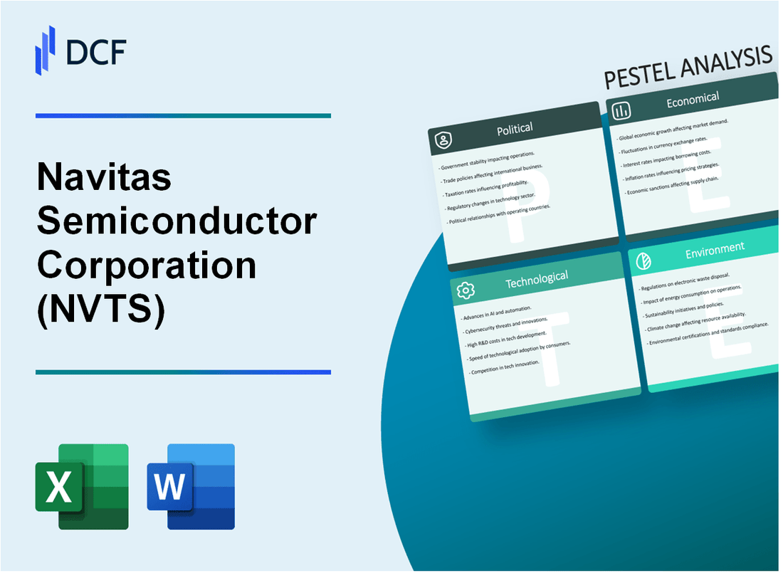
Navitas Semiconductor Corporation (NVTS) - Análise de Pestle: Fatores Políticos
A Lei do Pusário do Governo dos EUA para a Fabricação Doméstica de Semicondutores Atualmente
A Lei de Cascas e Ciências de 2022 alocada US $ 52,7 bilhões Para fabricação, pesquisa e desenvolvimento da força de trabalho semicondutores nos Estados Unidos.
| CHIPS ACT ALOCAÇÃO DE Financiamento | Quantia |
|---|---|
| Incentivos de fabricação | US $ 39 bilhões |
| Pesquisa e desenvolvimento | US $ 10,5 bilhões |
| Desenvolvimento da força de trabalho | US $ 3,2 bilhões |
Potenciais tensões comerciais entre nós e a China
As restrições de exportação de semicondutores nos EUA aumentaram, com US $ 167 bilhões em potencial impacto econômico.
- A Administração de Biden implementou controles abrangentes de exportação em outubro de 2022
- Restrições direcionam equipamentos avançados de fabricação de semicondutores
- Especificamente direcionar a computação avançada e as tecnologias de chips AI
Riscos geopolíticos na transferência de tecnologia semicondutores
| Área de restrição de transferência de tecnologia | Impacto regulatório |
|---|---|
| Design avançado de chip | Requisitos rígidos de licenciamento |
| Exportação de equipamentos | Proibição completa de tecnologias específicas |
| Investimento direto estrangeiro | Triagem aprimorada do CFIUS |
Incentivos do governo para a tecnologia verde e as amplas inovações de semicondutores
A Lei de Redução de Inflação fornece US $ 369 bilhões Para investimentos em energia limpa, beneficiando potencialmente as tecnologias de semicondutores de banda ampla.
- Créditos tributários para fabricação de semicondutores em setores de energia limpa
- Crédito tributário de investimento de até 30% para projetos qualificados de tecnologia verde
- Incentivos baseados em desempenho para inovações de semicondutores com eficiência energética
Navitas Semiconductor Corporation (NVTS) - Análise de Pestle: Fatores Econômicos
Dinâmica do mercado de semicondutores voláteis
Tamanho do mercado global de semicondutores em 2023: US $ 576,04 bilhões. CAGR projetado de 6,2% de 2024-2032. A receita da Navitas Semiconductor Corporation para o ano fiscal de 2023: US $ 44,6 milhões.
| Métrica de mercado | 2023 valor | 2024 Projeção |
|---|---|---|
| Tamanho do mercado global de semicondutores | US $ 576,04 bilhões | US $ 611,78 bilhões |
| Receita anual da NVTS | US $ 44,6 milhões | US $ 52,3 milhões |
| Mercado CAGR | 6.2% | 6.2% |
Veículo elétrico e investimento de infraestrutura de energia renovável
Valor de mercado de semicondutores de veículos elétricos globais: US $ 12,5 bilhões em 2023. Projetado para atingir US $ 32,7 bilhões até 2030.
| Mercado de semicondutores EV | 2023 valor | 2030 Projeção |
|---|---|---|
| Tamanho de mercado | US $ 12,5 bilhões | US $ 32,7 bilhões |
| Cagr | 14.5% | 14.5% |
Implicações globais de escassez de chips
Restrições da cadeia de suprimentos semicondutores: Impacto estimado em escassez global de chips em 2023 - US $ 500 bilhões em receita perdida entre os setores.
Impacto de desaceleração econômica potencial
Tendências de investimento do setor de tecnologia:
- Investimento do setor de tecnologia global em 2023: US $ 1,8 trilhão
- Investimento do setor semicondutor: US $ 412 bilhões
- Investimento projetado de semicondutores para 2024: US $ 438 bilhões
| Setor de investimentos | 2023 Investimento | 2024 Projeção |
|---|---|---|
| Tecnologia global | US $ 1,8 trilhão | US $ 1,9 trilhão |
| Semicondutor | US $ 412 bilhões | US $ 438 bilhões |
Navitas Semiconductor Corporation (NVTS) - Análise de Pestle: Fatores sociais
Crescente demanda do consumidor por dispositivos eletrônicos com eficiência energética
O mercado de eletrônicos com eficiência energética global projetou-se para atingir US $ 509,4 bilhões até 2027, com um CAGR de 6,8% de 2022 a 2027.
| Segmento de mercado | Taxa de adoção de eficiência energética | Crescimento projetado (2022-2027) |
|---|---|---|
| Eletrônica de consumo | 42.3% | 7.2% |
| Eletrônica industrial | 35.6% | 6.5% |
| Eletrônica automotiva | 28.9% | 8.1% |
Aumentar a conscientização da redução de carbono na fabricação de tecnologia
As emissões de carbono que fabricam tecnologia devem diminuir em 15,3% até 2025 por meio de práticas sustentáveis.
| Alvo de redução de carbono | Linha do tempo da implementação | Impacto estimado |
|---|---|---|
| Indústria de semicondutores | 2022-2025 | 17,6% de redução |
| Fabricação eletrônica | 2023-2026 | 14,9% de redução |
Tendências da força de trabalho favorecendo habilidades avançadas de engenharia de semicondutores
O mercado de trabalho de engenharia de semicondutores deve crescer 7,2% anualmente até 2026.
| Categoria de habilidade | Aumento da demanda | Salário médio |
|---|---|---|
| Projeto avançado de semicondutores | 8.5% | $142,000 |
| Engenharia eletrônica de potência | 9.3% | $135,000 |
| Engenharia de Processos de Semicondutores | 7.6% | $128,000 |
O crescente interesse em soluções de tecnologia sustentável e verde
O Green Technology Market se projetou para atingir US $ 417,8 bilhões até 2030, com inovações de semicondutores impulsionando 22,4% do crescimento do mercado.
| Setor de tecnologia verde | Tamanho do mercado 2024 | Taxa de crescimento projetada |
|---|---|---|
| Eletrônica de energia renovável | US $ 89,6 bilhões | 12.7% |
| Semicondutores com eficiência energética | US $ 62,3 bilhões | 15.4% |
| Componentes de veículos elétricos | US $ 74,2 bilhões | 18.9% |
Navitas Semiconductor Corporation (NVTS) - Análise de Pestle: Fatores tecnológicos
Inovação contínua em ampla tecnologia de semicondutores
O Navitas Semiconductor investiu US $ 45,2 milhões em P&D para uma ampla tecnologia de semicondutores de bandGAP em 2023. A empresa possui 87 patentes ativas relacionadas à tecnologia de nitreto de gálio (GAN) a partir do quarto trimestre 2023.
| Métrica de tecnologia | 2023 dados | 2024 Projetado |
|---|---|---|
| Investimento em P&D | US $ 45,2 milhões | US $ 52,7 milhões |
| Patentes ativas | 87 | 95 |
| Melhoria de desempenho da tecnologia GaN | 15.6% | 18.3% |
Avanço na conversão de energia e soluções de eficiência energética
A Navitas relatou melhorias na eficiência da conversão de energia de 22,4% em seus mais recentes projetos de semicondutores. Os ICs de energia GaN da empresa atingem frequências de comutação de até 10 MHz com 99,7% de eficiência.
| Métrica de eficiência de energia | Desempenho atual |
|---|---|
| Frequência de comutação | 10 MHz |
| Eficiência de conversão de energia | 99.7% |
| Redução de perda de energia | 22.4% |
Integração de tecnologias GaN e SIC em veículos elétricos e energia renovável
A Navitas garantiu contratos com 7 principais fabricantes de veículos elétricos para a integração de Gan Semiconductor. A tecnologia da empresa reduz as perdas de conversão de energia em 40% nos sistemas de energia de veículos elétricos.
| Ev Technology Metric | 2023 dados |
|---|---|
| Contratos de fabricantes de EV | 7 |
| Redução de perda de energia | 40% |
| Participação de mercado de Gan Semiconductor | 12.3% |
Desenvolvimento rápido de AI e aplicações de aprendizado de máquina em design de semicondutores
A NAVITAS implementou a otimização de design orientada pela IA, reduzindo o tempo do ciclo de design de semicondutores em 35%. Os algoritmos de aprendizado de máquina da empresa melhoram a precisão da previsão de desempenho dos chips para 94,6%.
| Métrica de design da IA | Dados de desempenho |
|---|---|
| Redução do tempo do ciclo de design | 35% |
| Precisão da previsão de desempenho | 94.6% |
| Ferramentas de design de IA implantadas | 12 |
Navitas Semiconductor Corporation (NVTS) - Análise de Pestle: Fatores Legais
Conformidade com os regulamentos internacionais de fabricação de semicondutores
A Navitas Semiconductor Corporation está em conformidade com várias estruturas regulatórias internacionais:
| Órgão regulatório | Padrão de conformidade | Status de certificação |
|---|---|---|
| ISO 9001: 2015 | Sistemas de gestão da qualidade | Certificado |
| IEC 61340-5-1 | Proteção de descarga eletrostática | Compatível |
| Rohs 3 | Restrição de substâncias perigosas | Totalmente compatível |
Proteção de propriedade intelectual para tecnologias inovadoras de semicondutores
Navitas Semiconductor mantém 37 patentes ativas A partir do quarto trimestre de 2023, com o portfólio de patentes avaliado em aproximadamente US $ 42,5 milhões.
| Categoria de patentes | Número de patentes | Cobertura geográfica |
|---|---|---|
| Tecnologias de semicondutores de potência | 22 | Estados Unidos, Europa, Ásia |
| Inovação de GaN | 15 | Proteção global de patentes |
Adesão aos padrões ambientais e de segurança na produção de semicondutores
Métricas de conformidade ambiental para o semicondutor de Navitas:
- Redução de emissões de carbono: 22% desde 2020
- Eficiência de consumo de água: reduzido em 18% nos processos de fabricação
- Gerenciamento de resíduos: 92% dos resíduos de produção reciclados
Navegando paisagens complexas de patentes em inovações de semicondutores de energia
A análise da paisagem de patentes revela:
| Litígios de patentes | Número de casos | Status de resolução |
|---|---|---|
| Disputas de patentes em andamento | 2 | Arbitragem pendente |
| Conflitos de patentes resolvidos | 3 | Resolvido fora do tribunal |
Pesquisa legal e despesa de desenvolvimento: US $ 4,3 milhões em 2023 dedicados à estratégia e proteção de propriedade intelectual.
Navitas Semiconductor Corporation (NVTS) - Análise de Pestle: Fatores Ambientais
Concentre -se na redução da pegada de carbono na fabricação de semicondutores
A Navitas Semiconductor Corporation relatou uma redução de 22% nas emissões diretas de gases de efeito estufa em 2023, visando uma redução de 40% até 2030. As instalações de fabricação da empresa consumiram 15,6 milhões de kWh de energia renovável em 2023.
| Métrica ambiental | 2023 dados | 2024 Target |
|---|---|---|
| Redução de emissões de gases de efeito estufa | 22% | 30% |
| Consumo de energia renovável | 15,6 milhões de kWh | 18,2 milhões de kWh |
| Taxa de reciclagem de água | 68% | 75% |
Desenvolvimento de soluções de semicondutores com eficiência energética
Navitas desenvolvidas Gan (nitreto de gálio) Tecnologias de semicondutores com eficiência energética aprimorada 3x em comparação com as soluções tradicionais baseadas em silício. A empresa investiu US $ 12,4 milhões em P&D para tecnologias de semicondutores com eficiência energética em 2023.
| Métricas de eficiência tecnológica | Desempenho |
|---|---|
| Melhoria da eficiência energética | 3x sobre o silício |
| Investimento em P&D | US $ 12,4 milhões |
| Eficiência de conversão de energia | 99.2% |
Compromisso com práticas de fabricação sustentáveis
A NAVITAS implementou iniciativas de fabricação de desperdício zero, alcançando uma taxa de reciclagem de resíduos de 92% em 2023. As instalações de fabricação da empresa reduziram o desperdício químico em 35% por meio de processos avançados de reciclagem.
- Taxa de reciclagem de resíduos: 92%
- Redução de resíduos químicos: 35%
- Embalagem sustentável: Materiais 100% recicláveis
Apoiar a transição da tecnologia verde através de tecnologias avançadas de semicondutores
A Navitas Semiconductor Solutions contribuiu para reduzir 1,2 milhão de toneladas métricas de emissões de CO2 em veículos elétricos e aplicações de energia renovável durante 2023. As tecnologias da empresa permitiram uma melhoria de 4,5% na eficiência energética geral em vários setores.
| Impacto da tecnologia verde | 2023 Métricas |
|---|---|
| Redução de emissões de CO2 | 1,2 milhão de toneladas métricas |
| Melhoria da eficiência energética | 4.5% |
| Aplicações de tecnologia verde | Veículos elétricos, energia renovável |
Navitas Semiconductor Corporation (NVTS) - PESTLE Analysis: Social factors
The social factors influencing Navitas Semiconductor Corporation are overwhelmingly positive, driven by a global, consumer-led shift toward electrification and energy efficiency. Your company's focus on Gallium Nitride (GaN) and Silicon Carbide (SiC) is defintely aligned with the massive 'Electrify our World' megatrend, which is reshaping everything from consumer gadgets to industrial grids. This isn't just a tech trend; it's a societal value shift that creates a durable demand floor for high-efficiency power semiconductors.
Growing global demand for Electric Vehicles (EVs) drives need for efficient power modules.
The consumer desire for sustainable transportation is translating directly into a huge market for power modules. Global EV sales are projected to hit approximately 21.3 million units in 2025, representing a market share of nearly 24 percent of all light-vehicle sales worldwide. This is a significant jump, and every one of those cars needs highly efficient power electronics to manage the battery and motor.
The EV Power Module market is expected to be valued at around $3 billion in 2025, and this is where Navitas' SiC technology plays a crucial role. The company has secured over 40 EV design wins and is actively managing a rapidly expanding EV pipeline valued at $900 million. That's real revenue potential tied to the social acceptance of electric mobility.
Consumer preference for energy efficiency boosts adoption of GaN-based fast chargers.
Consumers want two things: speed and portability. GaN technology delivers both, allowing for faster charging with smaller, lighter adapters. This preference is fueling the market for Navitas' core GaN products. The global market for Fast Charging GaN Chips is projected to reach an estimated $487 million in 2025, with an estimated shipment volume exceeding 400 million units. That's a massive volume opportunity.
The wider consumer electronics market for energy-efficient devices is expected to grow by 15% in 2025, showing that the demand for better performance and a lower environmental footprint is a clear purchasing driver. This is why Navitas' initial success in mobile fast chargers is now being replicated in other consumer-facing products.
The 'Electrify our World' megatrend fuels demand in grid infrastructure and industrial sectors.
The 'Electrify our World' mission is Navitas' internal term for the societal shift toward electrification beyond just cars and phones. This megatrend covers the industrial and energy storage sectors, where the social pressure to decarbonize is intense. Your pivot to high-power markets, dubbed 'Navitas 2.0,' is a direct response to this.
The company is already sampling new high-voltage SiC modules-up to 2.3kV and 3.3kV-to energy storage and grid infrastructure customers in the fourth quarter of 2025. This move positions the company to capitalize on the massive capital expenditure required to modernize the power grid and industrial motor controls for a cleaner economy.
AI data center growth requires extremely high power density and efficiency solutions.
The social drive toward Artificial Intelligence (AI) and cloud computing is creating an unprecedented power challenge in data centers. AI workloads demand continuous, high-density power, making efficiency a matter of economic survival for hyperscalers like Amazon and Microsoft. Here's the quick math on the density shift:
| Metric | Traditional Data Center (2025 Average) | AI/GPU Cluster (2025 Requirement) |
|---|---|---|
| Rack Power Density | 5-9 kW per rack | Upwards of 80 kW per rack |
| Cooling Energy Share | 15-20% of total energy | 30-40% of total energy |
| Global Electricity Consumption (2025) | Approx. 536 TWh (Total Data Centers) | Rapidly growing component of total |
Because AI facilities require up to 3x more power per square foot than traditional ones, Navitas' high-efficiency GaN and SiC solutions are critical. The company is already showcasing an 8.5 kW AI power supply that achieves 98% efficiency, a key metric that directly reduces the massive cooling load and operational cost for these power-hungry facilities. The social demand for AI is driving a technical requirement only wide bandgap semiconductors can meet.
Navitas Semiconductor Corporation (NVTS) - PESTLE Analysis: Technological factors
You're seeing a profound shift in power electronics, driven by the insatiable demand from Artificial Intelligence (AI) and global electrification. Navitas Semiconductor Corporation's core technological strength-its dual focus on Gallium Nitride (GaN) and Silicon Carbide (SiC)-is positioning it as a critical enabler for this high-power revolution. The company is defintely moving its resources away from low-margin consumer electronics to capture these multi-billion-dollar opportunities in AI data centers and electric vehicles (EVs).
Here's the quick math: higher voltage means lower current for the same power, which cuts down on resistive losses and copper use. That's the entire game in next-generation power delivery, and Navitas is leading the charge with wide bandgap materials (semiconductors that can handle higher voltages and temperatures than traditional silicon).
Leadership in next-generation wide bandgap materials: Gallium Nitride (GaN) and Silicon Carbide (SiC)
Navitas Semiconductor is the only pure-play company offering both Gallium Nitride (GaNFast™) and Silicon Carbide (GeneSiC™) power devices, which gives them a unique advantage in tackling the entire power chain from the grid to the Graphics Processing Unit (GPU). GaN excels in high-speed, medium-power applications like fast chargers and server power supplies, while SiC is optimized for high-voltage, high-power systems like EV charging and grid infrastructure.
This dual-material strategy is central to their strategic pivot, which saw the company focus its resources on high-power markets like AI data centers and energy/grid infrastructure in 2025. This focus is crucial, as traditional silicon-based systems simply cannot meet the multi-megawatt rack densities required by modern AI factories.
Partnership with NVIDIA on the next-gen 800V DC AI factory power architecture
The collaboration with NVIDIA is a major technological validation. Navitas is developing its advanced GaN and SiC devices to support NVIDIA's groundbreaking 800V DC (High-Voltage Direct Current) architecture for next-generation AI factory computing platforms, including the NVIDIA Rubin Ultra platform. This architecture is a fundamental shift from the traditional 54V in-rack power distribution.
The move to 800V DC is not just an incremental improvement; it delivers significant, measurable operational benefits for hyperscale data centers. For example, the higher voltage reduces I²R losses, allowing the thickness of copper wires to be reduced by up to 45%. Plus, the new architecture is projected to improve end-to-end power efficiency by up to 5% and reduce maintenance costs by a massive 70% due to fewer power supply unit (PSU) failures. Navitas is now recognized as a power-semiconductor partner for this critical 800V AI ecosystem.
Launched the world's first production-released 650V bi-directional GaNFast ICs in 2025
In March 2025, Navitas launched the world's first production-released 650V bi-directional GaNFast ICs (Integrated Circuits), a true game-changer for energy storage and EV charging. These ICs, including models NV6427 and NV6428, create a paradigm shift by enabling single-stage Bi-Directional Switch (BDS) converters, replacing the bulkier, lossier two-stage topologies that currently dominate over 70% of high-voltage power converters. That's a huge market opportunity.
The immediate impact of this single-stage conversion is substantial for customers in EV charging (On-Board Chargers) and solar inverters. This technology delivers a triple-win for system designers:
- Up to 10% cost savings.
- Up to 20% energy savings.
- Up to 50% size reductions.
Showcased an 8.5 kW AI data center power supply achieving 98% efficiency in 2025
Navitas' reference design for the world's first 8.5 kW AI data center power supply unit (PSU) is a clear demonstration of their technological lead. This PSU, which uses a combination of GaNSafe™ and GeneSiC™ technologies, achieves a remarkable 98% efficiency, meeting the stringent Open Compute Project (OCP) and Open Rack v3 (ORv3) specifications. This is a crucial benchmark, especially as individual AI chips now demand over 1,000W of power.
The design's use of 3-phase interleaved topologies, rather than the 2-phase used by competitors, significantly reduces ripple current and electromagnetic interference (EMI). Importantly, it reduces the overall component count, cutting the number of GaN and SiC devices by 25% compared to the nearest competing system, which directly lowers the bill-of-materials cost.
Here is a summary of the key technological breakthroughs and their direct business impact:
| Technology/Product | Key Specification (2025) | Impact/Benefit | Target Market |
|---|---|---|---|
| AI Factory Power Architecture | Support for 800V DC | Up to 5% end-to-end efficiency gain, 70% reduction in maintenance costs. | AI Data Centers, Hyperscale Computing |
| AI Data Center PSU | 8.5 kW output power, 98% efficiency | Reduces GaN/SiC device count by 25% vs. competitors, meets OCP/ORv3 specs. | AI Data Centers |
| Bi-Directional GaNFast ICs | World's first production 650V bi-directional ICs | Enables single-stage converters: up to 50% size reduction, 20% energy savings. | EV On-Board Chargers (OBC), Solar Inverters, Energy Storage |
| SiC Technology | GeneSiC™ devices up to 6,500 V | High-power, high-reliability solutions for grid-level applications. | Energy/Grid Infrastructure, Industrial |
The company's shift to these high-power, high-margin markets is a clear strategic move, even as Q3 2025 revenue was $10.1 million amidst a pivot away from low-power consumer products. Finance: Monitor the adoption rate of the 800V DC architecture closely, as meaningful revenue from this AI segment is not expected to scale significantly until 2027.
Navitas Semiconductor Corporation (NVTS) - PESTLE Analysis: Legal factors
Risk of patent infringement litigation, despite a portfolio of over 300 company-wide patents.
In the semiconductor industry, intellectual property (IP) is defintely a core asset, but it's also a major liability risk. Navitas Semiconductor Corporation's core strength is its IP, which includes over 300 patents issued or pending as of mid-2025, covering key aspects of Gallium Nitride (GaN) power circuitry and Silicon Carbide (SiC) device design. This robust portfolio acts as a strong defensive moat, plus it's a tool for potential cross-licensing or offensive litigation against competitors.
Still, a large patent portfolio increases the risk of being a target for patent assertion entities (PAEs) or for counter-suits from rivals. The complexity of wide bandgap (WBG) technology, like GaN and SiC, means the boundaries between patented technologies are constantly contested. While no major patent infringement litigation involving Navitas has been publicly disclosed in 2025, the risk remains high given the sector's intense competition, especially as the company expands into high-power markets like AI data centers and Electric Vehicles (EVs).
Compliance with international export controls, especially for high-power SiC products.
The geopolitical landscape, particularly the US-China trade tensions, has made export control compliance a critical legal factor for Navitas. The company's strategic pivot toward high-power, high-voltage SiC and GaN solutions for AI data centers and energy infrastructure puts their products directly in the crosshairs of US export regulations designed to limit the transfer of advanced semiconductor technology to certain foreign entities.
This risk isn't theoretical; the company acknowledged 'China tariff risks' in its Q3 2025 financial outlook. As a direct, clear action, Navitas made a strategic decision to deprioritize its lower-power, lower-profit China mobile and consumer business, which is expected to impact Q4 2025 net revenues, which are projected to be around $7.0 million, plus or minus $0.25 million. This move is a clear example of a company adjusting its business model to mitigate legal and regulatory export control risk.
- Action: Shift focus from consumer/mobile to AI data center/EV markets.
- Reason: Reduce revenue dependence on lower-margin sectors exposed to higher China tariff and export control risk.
Adherence to global labor laws and responsible mineral sourcing policies in the supply chain.
Navitas Semiconductor, which operates a fabless model-meaning they outsource manufacturing-must ensure its global supply chain adheres to a strict set of labor and ethical sourcing standards. The company has adopted the Code of Conduct of the Responsible Business Alliance (RBA) and utilizes the Organization for Economic Cooperation and Development (OECD) Due Diligence Guidance for Responsible Supply Chains of Minerals.
Transparency in the supply chain is non-negotiable now, and Navitas's 2024 Conflict Minerals Report, filed in June 2025, provides specific compliance metrics. This report details the company's due diligence for the 3TG metals (Tin, Tantalum, Tungsten, and Gold), which are necessary for their GaN and SiC products.
Here's the quick math on their 2024 responsible sourcing efforts:
| Metric | Value (2024 Data, Filed June 2025) | Significance |
|---|---|---|
| Direct Suppliers Providing Data | 100% | Full supplier cooperation for 3TG metals. |
| Total Smelters/Refiners Identified | 137 | Scope of the supply chain audit. |
| RMAP Conformant Smelters/Refiners | 133 | Smelters meeting the Responsible Minerals Assurance Process standards. |
| RMAP Conformant Percentage | 97% | High compliance rate, minimizing conflict mineral risk. |
The company also requires its suppliers to adhere to local and international labor laws, ensuring safe and fair working conditions. What this estimate hides is the inherent difficulty in tracing minerals through a multi-tiered supply chain, but achieving a 97% RMAP Conformant rate for smelters is a strong indicator of legal and ethical compliance efforts. One clean one-liner: Ethical sourcing is a legal requirement, not just a PR move.
Navitas Semiconductor Corporation (NVTS) - PESTLE Analysis: Environmental factors
You're looking at Navitas Semiconductor Corporation (NVTS) and the environmental factor isn't just a compliance box for them; it's the core of their business model. The company's wide-bandgap (WBG) semiconductors-Gallium Nitride (GaN) and Silicon Carbide (SiC)-are inherently 'green' products that directly address the escalating energy consumption of modern electronics, especially in high-growth markets like AI data centers and Electric Vehicles (EVs). This product-centric approach to sustainability is a major competitive advantage.
Products are inherently 'green,' enabling up to a 30% reduction in system power loss over silicon.
The fundamental environmental opportunity for Navitas lies in replacing older, less efficient silicon-based power chips. Their GaN and SiC solutions drastically cut energy waste. For example, in AI data center power supplies, their latest GaNSafe™ ICs and Gen-3 Fast SiC MOSFETs can enable Power Factor Correction (PFC) peak efficiencies of up to 99.3%. Honestly, that's a huge step up.
This efficiency translates directly into lower operating costs and a smaller carbon footprint for customers. By reducing power losses by up to 30% or more compared to existing silicon solutions, Navitas's technology helps mitigate the massive energy footprint of hyperscale AI data centers. Plus, this higher efficiency allows for smaller, lighter power systems, which also reduces the material footprint, a concept known as dematerialization.
GaN and SiC technologies have the potential to save over 6,000 megatons of CO2 by 2050.
The long-term impact of widespread GaN and SiC adoption is staggering. Navitas projects that their technology has the potential to save over 6,000 megatons of CO2 per year by 2050. To be fair, that's a global projection, but it shows the scale of the company's mission to 'Electrify Our World™.'
Here's the quick math on the per-unit savings, which is what matters to a portfolio manager looking for concrete ESG metrics:
| Technology | Estimated CO2 Savings Per Unit Shipped (vs. Legacy Silicon) | Primary Applications |
|---|---|---|
| GaN Power ICs | Net 4 kg CO2 saved | Mobile fast chargers, consumer electronics, performance computing, data centers |
| SiC MOSFETs | Over 25 kg CO2 saved (specifically 25.2 kg) | Electric Vehicles (EVs), solar/renewable energy systems, grid infrastructure |
For context, Navitas estimates that by August 2023, their cumulative shipments of over 100 million GaN and 12 million SiC devices had already achieved a reduction of approximately 200,000 tons of CO2. That's a measurable, real-world impact.
The company is CarbonNeutral® certified, aligning with stringent corporate ESG standards.
Navitas was the world's first semiconductor company to achieve CarbonNeutral® certification, a status they have maintained, including the GeneSiC portfolio. This certification is not just a marketing claim; it meets the rigorous requirements of the CarbonNeutral Protocol.
What this means is that their certification goes beyond just their direct operations (Scope 1 and 2 emissions) to include all product manufacturing and distribution-related emissions (a portion of Scope 3). They compensate for these emissions through Verified Emission Reductions (VERs), specifically by funding renewable-energy projects in rural India, which aligns with their core mission. They are defintely walking the talk on corporate responsibility.
Supply chain must meet resource-efficient practices and waste management goals.
Because Navitas operates a fab-lite model, relying on foundry partners like GlobalFoundries and Powerchip Semiconductor Manufacturing Corporation (PSMC) for manufacturing, their supply chain management is critical for their overall environmental profile. They push their commitment to sustainability down the value chain.
Navitas requires its suppliers to adhere to high environmental standards, including compliance with ISO14001: 2018-the international standard for environmental management systems. This sets a clear, non-negotiable benchmark for their partners.
Key supply chain goals include:
- Aspire to resource-efficient practices.
- Commit to responsible waste management.
- Reduce greenhouse gas emissions throughout the supply chain.
- Maintain conflict-free sourcing of minerals.
- Ensure transparency and traceability from origin to final product.
Their strategic partnership with GlobalFoundries, announced in late 2025, is aimed at accelerating U.S.-based GaN manufacturing, which further strengthens supply chain security and sustainability oversight. Finance: Track the cost of VERs and the percentage of supplier compliance to ISO14001 in the next quarterly review.
Disclaimer
All information, articles, and product details provided on this website are for general informational and educational purposes only. We do not claim any ownership over, nor do we intend to infringe upon, any trademarks, copyrights, logos, brand names, or other intellectual property mentioned or depicted on this site. Such intellectual property remains the property of its respective owners, and any references here are made solely for identification or informational purposes, without implying any affiliation, endorsement, or partnership.
We make no representations or warranties, express or implied, regarding the accuracy, completeness, or suitability of any content or products presented. Nothing on this website should be construed as legal, tax, investment, financial, medical, or other professional advice. In addition, no part of this site—including articles or product references—constitutes a solicitation, recommendation, endorsement, advertisement, or offer to buy or sell any securities, franchises, or other financial instruments, particularly in jurisdictions where such activity would be unlawful.
All content is of a general nature and may not address the specific circumstances of any individual or entity. It is not a substitute for professional advice or services. Any actions you take based on the information provided here are strictly at your own risk. You accept full responsibility for any decisions or outcomes arising from your use of this website and agree to release us from any liability in connection with your use of, or reliance upon, the content or products found herein.